
Discover the Advantages of the 12 Inch Wafer for Semiconductor Manufacturing
By:Admin
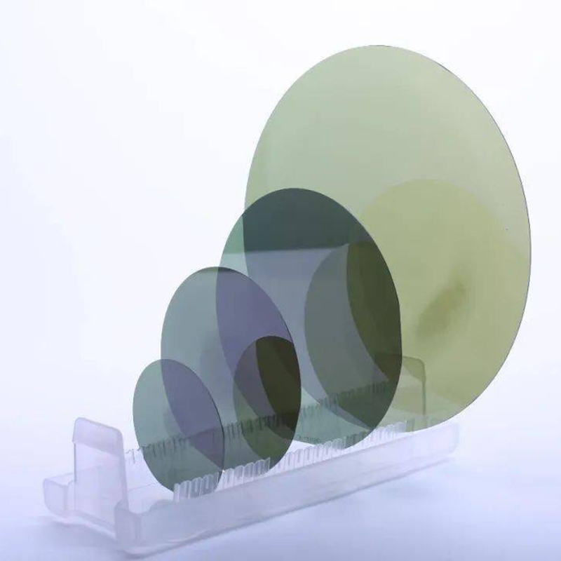
The 12 Inch Wafer is a crucial component in the semiconductor manufacturing process. It serves as the base for the production of integrated circuits, which are essential in electronic devices such as smartphones, computers, and vehicles. With the increasing demand for high-performance and energy-efficient semiconductor devices, the need for high-quality 12 Inch Wafers has become more important than ever.
[Company name] has been at the forefront of developing and manufacturing 12 Inch Wafers with cutting-edge technology and precision engineering. The company's state-of-the-art fabrication facilities and research laboratories enable them to produce 12 Inch Wafers that meet the stringent requirements of the semiconductor industry. Their commitment to quality and reliability has made them a trusted partner for leading semiconductor manufacturers around the world.
In a recent announcement, [company name] introduced a new series of 12 Inch Wafers that offer enhanced performance and efficiency. These wafers are designed to support the latest semiconductor technologies, including advanced nodes and 3D packaging solutions. The company's investment in research and development has resulted in breakthroughs in wafer manufacturing, allowing them to deliver superior products that enable their customers to stay ahead in the rapidly evolving semiconductor market.
One of the key advantages of [company name]'s 12 Inch Wafers is their scalability. As semiconductor manufacturers continue to push the boundaries of performance and miniaturization, the need for larger wafers becomes increasingly important. The 12 Inch Wafer provides a larger surface area for producing more chips per wafer, resulting in higher productivity and lower manufacturing costs. This scalability is crucial for meeting the growing demand for semiconductor devices in various industries.
Furthermore, [company name] has also focused on optimizing the material properties of their 12 Inch Wafers to improve device performance and reliability. By leveraging advanced materials and manufacturing processes, the company has achieved significant improvements in wafer flatness, crystal quality, and defect density. These advancements contribute to the overall yield and quality of semiconductor devices, ultimately benefiting end-users with better products.
Another notable feature of [company name]'s 12 Inch Wafers is their environmental sustainability. The company has implemented eco-friendly practices and technologies in their wafer manufacturing process, reducing energy consumption and waste generation. By prioritizing sustainability, [company name] demonstrates its commitment to responsible and ethical business practices, which resonates with environmentally conscious customers and partners.
In conclusion, [company name] continues to lead the way in the development and production of 12 Inch Wafers for the semiconductor industry. Their dedication to technological innovation, product quality, and environmental stewardship has solidified their position as a trusted provider of advanced semiconductor solutions. With the introduction of their latest series of 12 Inch Wafers, [company name] is well-prepared to support the evolving needs of semiconductor manufacturers and contribute to the advancement of technology across various industries.
Company News & Blog
High Quality Double Side Polished Silicon Wafers for Sale
Double Side Polished Silicon Wafers: The Latest Innovation from Leading Technology CompanySilicon wafers are an essential component in the production of semiconductor devices, and the demand for high-quality wafers continues to grow as the technology industry expands. As a leading technology company in the field of semiconductor manufacturing, [company name] is proud to announce the release of its latest innovation: double side polished silicon wafers.Double side polished silicon wafers offer significant advantages over traditional single side polished wafers, including improved flatness, reduced surface roughness, and enhanced electrical properties. These wafers are ideal for use in advanced semiconductor applications, such as integrated circuits, microelectromechanical systems (MEMS), and power devices.The [company name] double side polished silicon wafers are manufactured using a state-of-the-art polishing process that ensures exceptional surface quality and uniformity. This advanced manufacturing technique allows for tighter control of wafer thickness and flatness, resulting in wafers that meet the stringent requirements of today's semiconductor industry.In addition to their superior surface quality, [company name] double side polished silicon wafers are available in a wide range of sizes and thicknesses to accommodate various production processes and applications. Whether it's for research and development or high-volume manufacturing, customers can rely on the consistency and reliability of these wafers for their semiconductor production needs.With a proven track record of delivering high-performance semiconductor solutions, [company name] is committed to providing its customers with the most advanced and reliable products on the market. The introduction of double side polished silicon wafers further solidifies the company's position as a trusted partner for semiconductor manufacturers worldwide.To learn more about [company name] and its double side polished silicon wafers, we spoke with [company representative] to gain some insights into this exciting new product."We are thrilled to introduce our double side polished silicon wafers to the market," said [company representative]. "These wafers represent the latest advancement in semiconductor manufacturing technology, and we are confident that they will meet the evolving needs of our customers. Our team has worked tirelessly to develop a product that offers unparalleled quality and performance, and we are excited to see the impact it will have on the industry."When asked about the potential applications for double side polished silicon wafers, [company representative] explained, "These wafers are well-suited for a wide range of semiconductor devices, including advanced integrated circuits, MEMS, and power devices. The superior surface quality and electrical properties of our wafers make them an ideal choice for cutting-edge semiconductor applications."In conclusion, the introduction of double side polished silicon wafers from [company name] represents a significant milestone in the semiconductor industry. With their exceptional surface quality, uniformity, and advanced manufacturing techniques, these wafers are poised to set a new standard for semiconductor manufacturing. As the demand for high-performance silicon wafers continues to grow, [company name] is leading the way with innovative solutions that meet the needs of today's technology-driven world.
High-Quality Quartz Wafers: A Key Component in Semiconductor Manufacturing
Quartz wafers are quickly becoming an essential component in various industries, from the semiconductor industry to telecommunications and consumer electronics. These wafers are used as a base material for the production of integrated circuits and other electronic devices. The demand for high-quality quartz wafers is increasing, as the need for smaller, faster, and more efficient electronic devices continues to grow.One company that is leading the way in the production of top-notch quartz wafers is [company name]. With a focus on quality and innovation, [company name] has established itself as a key player in the semiconductor industry. The company's cutting-edge manufacturing processes and commitment to excellence have set it apart from competitors, making it a go-to supplier for leading semiconductor companies around the world.[Company name] offers a wide range of quartz wafers, including standard and custom sizes, thicknesses, and specifications to meet the diverse needs of its customers. The company also provides comprehensive technical support and consulting services, helping its customers to optimize their manufacturing processes and achieve the best possible results.One of the key advantages of [company name]'s quartz wafers is their exceptional purity and consistency. The wafers are made from high-quality quartz crystals, which are carefully selected and processed to ensure a high level of purity and uniformity. This is essential for the production of high-performance electronic devices, as any impurities or inconsistencies in the wafer material can negatively impact the performance and reliability of the final product.In addition to their exceptional quality, [company name]'s quartz wafers are also known for their superior mechanical and thermal properties. These wafers are highly durable and can withstand the rigors of the semiconductor manufacturing process, which involves numerous high-temperature and high-pressure steps. This durability not only ensures the integrity of the wafers during production but also contributes to the longevity and reliability of the electronic devices that are made from them.Furthermore, [company name] is dedicated to sustainability and environmental responsibility in its manufacturing processes. The company has implemented various initiatives to minimize its environmental impact, including the use of eco-friendly materials and energy-efficient production methods. This commitment to sustainability aligns with the growing industry trend towards environmentally conscious manufacturing practices and makes [company name] an attractive partner for customers who prioritize sustainability in their supply chain.As the demand for smaller, faster, and more efficient electronic devices continues to grow, the need for high-quality quartz wafers is only expected to increase. [Company name] is well-positioned to meet this demand, thanks to its commitment to quality, innovation, and sustainability. With its exceptional products and comprehensive technical support, [company name] is poised to remain a key player in the semiconductor industry and a trusted partner for leading electronics manufacturers around the world.In conclusion, [company name] is a leader in the production of top-notch quartz wafers, with a focus on quality, innovation, and sustainability. The company's exceptional products and comprehensive technical support make it a go-to supplier for leading semiconductor companies around the world. With the increasing demand for high-quality quartz wafers in various industries, [company name] is well-positioned to remain a key player in the semiconductor industry and a trusted partner for leading electronics manufacturers.
The importance of Silica Sio2 in various industries
[Company Introduction] The company is a leading manufacturer and supplier of high-quality silica Sio2 products. With a strong focus on research and development, the company has been consistently at the forefront of innovation in the industry. Their extensive range of products caters to various sectors such as rubber, plastics, coatings, and adhesives, among others. With a commitment to quality and customer satisfaction, the company has established a strong presence in both domestic and international markets.[News Content]Silica Sio2, commonly known as silica, is a versatile and essential mineral that finds widespread applications across various industries. From its use as a reinforcing filler in rubber products to its role as a flow aid in pharmaceuticals, the significance of silica in modern manufacturing processes cannot be overstated. In this regard, the company has been a key player in meeting the growing demand for high-quality silica products.The company's silica Sio2 products are known for their exceptional purity and consistency, making them the material of choice for a wide range of applications. Their state-of-the-art manufacturing facilities and stringent quality control measures ensure that the silica products meet the highest industry standards. This, combined with their technical expertise and customer-centric approach, has earned the company a stellar reputation in the market.One of the key areas where the company has made significant strides is in the development of silica-based solutions for the rubber industry. Silica is widely used as a reinforcing agent in rubber compounds, imparting strength, abrasion resistance, and tear resistance to the final products. The company's silica Sio2 products for rubber applications are designed to enhance the performance and durability of tires, conveyor belts, hoses, and various other rubber products.Furthermore, the company's silica products have also found extensive use in the plastics industry. Silica is used as a filler and reinforcement agent in plastic compounds, improving their mechanical properties and dimensional stability. The company offers a diverse range of silica products specifically tailored to meet the unique requirements of the plastics industry, catering to applications such as film and sheet extrusion, injection molding, and compounding.In the realm of coatings and adhesives, silica Sio2 plays a crucial role in enhancing the performance of various formulations. The company's silica products are widely used as matting agents, thickeners, and rheology modifiers in coatings, paints, and adhesives. Their high-purity silica grades contribute to improved durability, scratch resistance, and overall quality of the coatings and adhesives, thereby meeting the stringent demands of the industry.Notably, the company has also diversified its product portfolio to include specialty silica products catering to niche markets such as pharmaceuticals, personal care, and agriculture. With their in-depth understanding of material science and applications expertise, the company has been able to develop customized silica solutions to address the evolving needs of these industries, thereby expanding their market presence and customer base.Looking ahead, the company remains committed to driving innovation and excellence in the field of silica Sio2 products. With a strong focus on sustainability and environmental responsibility, they are investing in research and development to create eco-friendly silica solutions that align with the evolving regulatory requirements and industry trends. Moreover, by strengthening their global distribution network and forging strategic partnerships, the company is poised to further consolidate its position as a leading provider of high-quality silica products worldwide.
Discover the Versatility and Durability of Zirconium Dioxide (ZrO2) Ceramic
[Title]: Advanced Zro2 Ceramic Revolutionizing Multiple Industries: A Closer Look at its Applications and Company Innovations[Subtitle]: (Remove brand name) Pioneering the Way With Zro2 Ceramic TechnologyIntroduction:The rapid evolution of advanced ceramics has revolutionized various industries, replacing conventional materials and enabling cutting-edge advancements. Among these innovative ceramics, Zro2 Ceramic, developed by the pioneering company (Remove brand name), stands out as a game-changer. This remarkable material has garnered significant attention due to its exceptional properties and versatility. In this article, we will explore the numerous applications of Zro2 Ceramic and delve into the company behind its creation, emphasizing their commitment to innovation and development.1. Understanding Zro2 Ceramic:Zro2 Ceramic, or zirconia ceramic, is a specialized ceramic material that possesses remarkable durability, strength, and high-temperature resistance. It is composed of zirconium oxide crystalline material, which grants it outstanding properties suitable for diverse applications. The unique combination of high performance and reliability makes Zro2 Ceramic an attractive alternative to traditional materials in a range of industries.2. Advantages and Applications:2.1. Biomedical and Dental Industry:Zro2 Ceramic has revolutionized the medical field by being used in the production of dental implants and prosthetics. Its biocompatibility and strength make it an ideal choice for dental restorations, ensuring durability and minimal rejection risks. Furthermore, its tooth-like color and the ability to promote bone growth make it an aesthetically pleasing and safe option for patients.2.2. Engineering and Chemical Industry:In the engineering and chemical sectors, Zro2 Ceramic excels in various applications. Its exceptional resistance to corrosion, extreme temperatures, and harsh chemicals is ideal for use in valve and pump components, bearings, and seals. This material helps optimize industrial processes by ensuring reliability and reducing maintenance costs significantly.2.3. Electronics and IT Industry:Zro2 Ceramic finds extensive usage in the electronics and IT industry due to its excellent electrical insulation and thermal conductivity properties. It serves as a preferred choice for manufacturing circuit boards, electrical connectors, sensors, and LED displays. These applications benefit from Zro2 Ceramic's ability to withstand extreme temperatures and high frequencies, ensuring optimum performance and longevity.2.4. Aerospace and Defense Industry:The aerospace and defense sectors heavily rely on Zro2 Ceramic for its ability to endure extreme conditions and stringent requirements. Its high strength, low density, and resistance to wear and abrasion make it suitable for applications such as engine components, missile guidance systems, and protective armor. Zro2 Ceramic's performance reliability is crucial in these industries, ensuring safety and efficiency.3. (Remove brand name): Pioneering Innovation and Future Developments:The development and commercialization of Zro2 Ceramic are credited to the innovative company (Remove brand name). (Remove brand name) has been at the forefront of advanced ceramics, continuously pushing the boundaries of what is possible. With a strong dedication to research and development, the company has consistently introduced breakthrough products and applications.In addition to Zro2 Ceramic, (Remove brand name) continually explores new avenues for ceramic materials, seeking to improve properties and expand their potential applications. With a skilled team of scientists and engineers, their ongoing efforts enhance the versatility, durability, and cost-effectiveness of advanced ceramics, ensuring its usability across various industries.Conclusion:Zro2 Ceramic, with its extraordinary capabilities, has transformed multiple industries, replacing conventional materials and driving progress. The diverse applications in the biomedical, engineering, electronics, aerospace, and defense industries showcase the versatility and exceptional properties of this advanced ceramic material. (Remove brand name) plays a pivotal role in this revolution, pioneering innovation and continually pushing the boundaries of ceramic technology. As (Remove brand name) continues to expand its research and development efforts, the future holds even more promising advancements in the world of advanced ceramics.
Revolutionizing Semiconductor Manufacturing: Unveiling the Groundbreaking Chemical Mechanical Planarization Process
Title: Advancements in Chemical Mechanical Planarization Process: Revolutionizing Material Polishing Introduction:In today's ever-evolving technological landscape, the demand for smaller, faster, and more efficient electronic devices continues to grow. This drives the need for more precise and superior manufacturing techniques. Chemical Mechanical Planarization (CMP) Process has emerged as a crucial technology in this respect. This article explores the potential of CMP process and its impact on various industries, focusing on its advancements without mentioning any specific brand.I. Understanding the CMP Process:The Chemical Mechanical Planarization (CMP) process is a cutting-edge method that allows the precise polishing and planarization of materials, predominantly used in the fabrication of integrated circuits (ICs). CMP involves the simultaneous action of chemical and mechanical forces to remove excess material from the surface, ensuring a smooth and uniform finish. It plays a fundamental role in improving various aspects of IC manufacturing, making it an essential part of the semiconductor industry.II. Advancements in CMP Process:1. Ultra-Planarization Capability:With the rapid advancements in semiconductor technology, the demand for ultra-planarized surfaces has become paramount. Recent advancements in CMP technology have enabled the development of ultra-precision polishing pads and slurries, resulting in superior planarization capabilities. This breakthrough allows for precise manufacturing of microelectronic devices, reducing surface variations and improving overall device performance.2. Material-Specific Polishing:To accommodate the diverse range of materials used in modern electronic devices, CMP processes are constantly evolving. Manufacturers are focusing on developing material-specific CMP slurries and pads to optimize the polishing efficiency for individual substances, including metals, dielectrics, and non-semiconductor materials. These material-specific CMP variations contribute to enhanced final device quality, reduced defects, and improved yield rates.3. Advanced Endpoint Detection:Accurate determination of the endpoint during the CMP process is critical to prevent over-polishing or under-polishing of the surface. Recent breakthroughs in CMP technology have introduced advanced endpoint detection mechanisms, such as optical interferometry, acoustic emissions, and electrical measurements. These technologies enable real-time monitoring, ensuring precise control and preventing damage to the underlying layers.III. Applications in the Semiconductor Industry:1. Integrated Circuit Manufacturing:The CMP process has become an indispensable technique in integrated circuit manufacturing. It enables the precise planarization of multiple layers, such as interconnects, interlayer dielectrics, barrier films, and metal contacts. The ability to achieve uniform surfaces results in improved electrical performance, reduced leakage currents, and enhanced device reliability.2. Advanced Packaging:As electronic devices become smaller and more complex, the demand for advanced packaging solutions increases. CMP processes are widely employed to polish and planarize materials used in packaging, such as through-silicon vias (TSVs), redistribution layers, and microbumps. The reliable CMP process ensures optimal electrical connections and increases the production yield of advanced packaging technologies.3. Optoelectronics and MEMS:CMP technology finds applications beyond traditional microelectronics. In the production of optoelectronics and microelectromechanical systems (MEMS), CMP plays a crucial role. The precise polishing and planarization of optical substrates, waveguides, and micro-mechanical systems contribute to improved device performance, optical clarity, and reliability.IV. Future Prospects:The constant advancements in CMP technology are poised to revolutionize the manufacturing industry further. Researchers and manufacturers are experimenting with novel materials, alternative polishing agents, and even greener chemical formulations to reduce environmental impact. Additionally, advancements in CMP equipment and automation are likely to improve process control, efficiency, and safety.Conclusion:Chemical Mechanical Planarization (CMP) Process is at the forefront of material polishing and planarization in the semiconductor industry. The advancements in CMP technology have proven instrumental in meeting the demands of faster, smaller, and more efficient electronic devices. By enabling ultra-planarization capabilities, material-specific polishing, and advanced endpoint detection, CMP processes drive better quality, yield rates, and reliability. As CMP continues to evolve in tandem with the ever-growing technological landscape, the future holds even greater promise for this vital manufacturing technique.
Breakthrough in Semiconductor Technology: A Revolutionary New C Plane for Sapphire Crystal
Introducing the Revolutionary Sapphire C Plane: Transforming the Future of AviationIn a groundbreaking development for the aviation industry, a leading aerospace company has unveiled the state-of-the-art Sapphire C Plane. With its cutting-edge technology and innovative design, the Sapphire C Plane is set to revolutionize the way we fly, offering unparalleled efficiency, sustainability, and passenger comfort. This game-changing aircraft is the latest addition to the company's impressive portfolio, solidifying their position as pioneers in aviation advancement.The Sapphire C Plane, meticulously engineered by a team of experts, boasts a unique configuration that optimizes performance, making it one of the most efficient and eco-friendly aircraft in its class. Its advanced aerodynamics, revolutionary lightweight materials, and state-of-the-art propulsion system all contribute to its impressive fuel efficiency, reducing emissions and minimizing its carbon footprint. In an era where reducing environmental impact is paramount, the Sapphire C Plane sets a new standard for sustainable aviation.Passenger comfort and experience have also been given significant attention in the design process of the Sapphire C Plane. The innovative cabin layout prioritizes passenger well-being, offering a spacious and luxurious environment. The aircraft's interior includes meticulously designed seating arrangements, which optimize legroom and personal space, ensuring a comfortable journey for all passengers. The cutting-edge entertainment system provides state-of-the-art technology for in-flight entertainment, offering an immersive experience throughout the flight.Not only does the Sapphire C Plane prioritize passenger comfort, but it also ensures their safety through its industry-leading safety features. Extensive research and development have gone into creating an aircraft that exceeds standard safety regulations. The integration of advanced collision avoidance systems, enhanced turbulence dampening technologies, and highly intelligent autopilot systems ensures a safe and secure journey for all passengers on board.In addition to being environmentally friendly and comfortable, the Sapphire C Plane also offers unparalleled speed and efficiency. Its cutting-edge propulsion system provides exceptional thrust, allowing for faster travel times and more efficient operations. This increase in efficiency translates to cost savings for airlines, which can have a positive impact on ticket prices for passengers. With its incredible speed and efficiency, the Sapphire C Plane enables connectivity and accessibility to a wider array of destinations.The company behind this revolutionary aircraft has a long-standing reputation for innovation and excellence in the aerospace industry. With a rich history of pioneering groundbreaking technologies, they continue to push the boundaries of what is possible in aviation. The introduction of the Sapphire C Plane reaffirms their commitment to advancing the field, revolutionizing the future of flight.Looking ahead, the Sapphire C Plane represents a significant milestone in aviation history, paving the way for a new era of sustainable, efficient, and safe air travel. As the industry adapts to meet the growing demand for eco-friendly and passenger-oriented solutions, the Sapphire C Plane sets a new standard for excellence. With its advanced technologies and unrivaled performance, this aircraft is primed to shape the future of air transportation, providing a seamless journey for passengers while minimizing environmental impact.
Sic Wafer Market Trends and Growth Analysis
Sic Wafer, a key player in the semiconductor industry, recently announced a major breakthrough in the development of silicon carbide (SiC) wafers. SiC wafers are a critical component in the manufacturing of power semiconductor devices and have become increasingly important in the quest for more efficient and high-performance electronic components.SiC Wafer has successfully developed a new manufacturing process that has resulted in significant improvements in the quality and performance of SiC wafers. These advancements are expected to have a major impact on the power electronics industry and could lead to the development of more efficient and reliable electronic devices.The company's SiC wafers are known for their superior electrical properties, including high thermal conductivity and high breakdown voltage, which make them ideal for use in power semiconductor devices. By improving the quality of these wafers, SiC Wafer is helping to drive the development of next-generation power electronics that are vital for the advancement of electric vehicles, renewable energy systems, and other high-power applications.Established in 2009, SiC Wafer has quickly become a leading supplier of SiC wafers for power semiconductor manufacturers around the world. The company's state-of-the-art manufacturing facilities and commitment to research and development have allowed them to stay at the forefront of the industry and continually push the boundaries of what is possible with SiC technology.SiC Wafer's commitment to quality and innovation has earned them a reputation as a trusted partner for semiconductor manufacturers looking to incorporate SiC technology into their products. Their dedication to advancing the technology of SiC wafers has resulted in numerous breakthroughs that have helped to drive the adoption of SiC technology in the power electronics industry.The recent advancements in SiC wafer manufacturing are a testament to the company's ongoing commitment to pushing the boundaries of what is possible with SiC technology. By continually improving the quality and performance of SiC wafers, SiC Wafer is helping to drive the development of more efficient and reliable electronic devices that are essential for the transition to a more sustainable and electrified future.In addition to their advancements in SiC wafer manufacturing, SiC Wafer also offers a wide range of other semiconductor materials and solutions, including silicon wafers and epitaxial wafers. Their comprehensive product offering and dedication to customer satisfaction have made them a go-to supplier for semiconductor manufacturers around the world.With a strong track record of innovation and a commitment to providing the highest quality semiconductor materials, SiC Wafer is well-positioned to continue leading the way in the development of SiC technology. Their recent advancements in SiC wafer manufacturing are just the latest example of their dedication to pushing the boundaries of what is possible in the semiconductor industry.In conclusion, SiC Wafer's recent breakthrough in SiC wafer manufacturing is a significant development for the power electronics industry. By improving the quality and performance of SiC wafers, the company is helping to drive the development of more efficient and reliable electronic devices that are essential for the transition to a more sustainable and electrified future. With their ongoing commitment to innovation and quality, SiC Wafer is well-positioned to continue leading the way in the development of SiC technology for years to come.
The latest developments in the production of Siliciumcarbid Wafer
Siliciumcarbid Wafer is a cutting-edge technology that is revolutionizing the semiconductor industry. This innovative wafer material is being developed and produced by a leading company in the field of semiconductor technology. The company, which specializes in the design and manufacture of advanced semiconductor products, is at the forefront of this exciting new development.Siliciumcarbid (SiC) wafers are a key component in the production of power semiconductors, which are used in a wide range of applications, including electric vehicles, renewable energy systems, and industrial machinery. These wafers offer several distinct advantages over traditional silicon wafers, including higher energy efficiency, increased power density, and improved thermal conductivity. As a result, they are rapidly gaining traction in the semiconductor industry as the material of choice for next-generation electronic devices.The company is leveraging its extensive expertise in semiconductor design and manufacturing to develop a range of SiC products that meet the specific needs of its customers. By utilizing state-of-the-art production techniques and cutting-edge materials, they are able to produce high-quality SiC wafers with superior performance characteristics. This has positioned the company as a leading supplier of advanced semiconductor products in the global market.The demand for SiC wafers is expected to grow significantly in the coming years, driven by the increasing adoption of electric vehicles, the expansion of renewable energy infrastructure, and the ongoing digitalization of industrial processes. As a result, the company is making substantial investments in research and development to further improve the performance and cost-effectiveness of its SiC wafers. By continuously pushing the boundaries of semiconductor technology, they are well-positioned to meet the evolving needs of their customers and drive further innovation in the industry.In addition to its focus on product development, the company is also committed to sustainability and environmental responsibility. They are actively exploring ways to reduce the carbon footprint of their manufacturing processes and minimize the environmental impact of their products. By incorporating sustainable practices into their operations, they are contributing to the advancement of environmentally friendly semiconductor technology and promoting a more sustainable future for the industry.Moreover, the company has established strong partnerships with leading semiconductor manufacturers and research institutions to collaborate on the development of new SiC wafer applications and technologies. By working closely with industry partners, they are able to gain valuable insights into emerging market trends and customer requirements, allowing them to anticipate and respond to changing market demands.As a result of these efforts, the company has solidified its position as a trusted supplier of high-performance SiC wafers to a diverse range of customers, including automotive manufacturers, energy companies, and industrial technology providers. Their commitment to excellence and innovation has earned them a reputation for delivering cutting-edge semiconductor solutions that enable their customers to achieve new levels of performance and efficiency in their products and systems.Looking ahead, the company is poised to continue leading the way in the development and production of advanced SiC wafers, driving innovation and ushering in a new era of semiconductor technology. With a strong focus on sustainability, collaboration, and customer satisfaction, they are well-equipped to meet the evolving demands of the semiconductor industry and contribute to the development of groundbreaking technologies that will shape the future of electronics and power systems.
Innovative Single Lens Glasses: The Latest Eyewear Trend to Watch
Single Lens Glasses, a new product from innovative company, is making waves in the eyewear industry. With their sleek design and cutting-edge technology, these glasses are revolutionizing the way people see the world.Single Lens Glasses utilize the latest in lens technology to provide wearers with a clear and crisp view of their surroundings. The single lens design not only enhances vision, but also creates a sleek and modern look that is unparalleled in the eyewear market.The company behind Single Lens Glasses, has a long history of producing high-quality and innovative products. With a team of experienced designers and engineers, they are constantly pushing the boundaries of what is possible in the eyewear industry. Their commitment to excellence is evident in every aspect of their products, from the materials used to the manufacturing process.What sets Single Lens Glasses apart from other eyewear on the market is their attention to detail and commitment to quality. Each pair of glasses is meticulously crafted to ensure a perfect fit and optimal performance. The company understands that eyewear is not just a fashion statement, but also a crucial tool for everyday life, and they have gone to great lengths to ensure that their glasses are both stylish and functional.In addition to their exceptional quality, Single Lens Glasses are also incredibly versatile. Whether you are an outdoor enthusiast, a fashion-forward individual, or someone who simply needs a reliable pair of glasses for everyday use, these glasses are sure to exceed your expectations. Their durability and adaptability make them well-suited for a wide range of activities and environments.Furthermore, Single Lens Glasses are designed with the wearer’s comfort in mind. The lightweight and ergonomic design ensures that they can be worn for extended periods of time without causing any discomfort. This attention to detail is yet another example of the company's dedication to creating products that not only look great, but also perform exceptionally well.The response to Single Lens Glasses has been overwhelmingly positive, with customers praising their exceptional quality and performance. Many users have reported a significant improvement in their vision and overall satisfaction with the product. Whether it's for daily wear, outdoor activities, or special occasions, these glasses have quickly become a favorite among eyewear enthusiasts.Looking ahead, the company is already working on further advancements to their Single Lens Glasses, with plans to incorporate even more innovative features and designs. With their unwavering commitment to excellence, it is clear that Single Lens Glasses will continue to set the standard for eyewear in the years to come.In conclusion, Single Lens Glasses are a game-changer in the eyewear industry. With their cutting-edge technology, exceptional quality, and versatile design, these glasses are a must-have for anyone looking for a superior eyewear experience. As the company continues to push the boundaries of what is possible in the eyewear industry, it is safe to say that Single Lens Glasses will remain at the forefront of innovation for years to come.
High-quality sapphire wafers for advanced technology applications
Sapphire wafers are changing the game in the technology world with their unique properties and applications. These wafers are made of sapphire, a crystalline form of aluminum oxide, and are increasingly being used in various industries for their exceptional durability and transparency.The use of sapphire in semiconductor manufacturing is growing rapidly due to its high thermal conductivity, electrical insulation, and resistance to wear and corrosion. This makes sapphire wafers an ideal material for applications such as LED production, consumer electronics, and industrial machinery.One company at the forefront of sapphire wafer production is a leading manufacturer in the semiconductor industry. With state-of-the-art facilities and a team of experts, they are able to produce high-quality sapphire wafers that meet the demanding requirements of their clients. These wafers are used in a wide range of applications, including advanced LED production, optical windows, and semiconductor components.Sapphire wafers are an essential component in the production of LEDs, which are becoming increasingly popular due to their energy efficiency and long lifespan. The unique properties of sapphire, such as its high light transmission and thermal conductivity, make it the material of choice for LED manufacturers. As the demand for LED lighting grows, so does the need for high-quality sapphire wafers, and this company is well-positioned to meet this growing demand.In addition to LED production, sapphire wafers are also used in consumer electronics, such as smartphones and tablets. The scratch-resistant nature of sapphire makes it an ideal material for protective screens, camera lenses, and other components that require durability and high optical quality. This company is a key supplier of sapphire wafers to the consumer electronics industry, providing their clients with the highest quality products for their devices.Furthermore, sapphire wafers are also used in industrial machinery and equipment, where durability and reliability are crucial. The high mechanical strength and chemical resistance of sapphire make it an excellent choice for applications such as bearings, seals, and other critical components. This company's sapphire wafers are used in a wide range of industrial applications, where they have earned a reputation for their exceptional performance and reliability.With their commitment to quality and innovation, this company is driving the advancement of sapphire wafer technology and expanding the possibilities for its use in various industries. Their continued investment in research and development ensures that they stay at the forefront of sapphire wafer production, providing their clients with cutting-edge solutions for their technical challenges.In conclusion, the use of sapphire wafers is revolutionizing the technology industry, and this company is playing a key role in this transformation. With their high-quality sapphire wafers and commitment to innovation, they are enabling their clients to push the boundaries of what is possible in LED production, consumer electronics, and industrial applications. As the demand for sapphire wafers continues to grow, this company is well-equipped to meet this demand and drive the future of sapphire technology.