
Durable and Heat-Resistant Quartz Glass: A Breakthrough Material for Various Applications
By:Admin
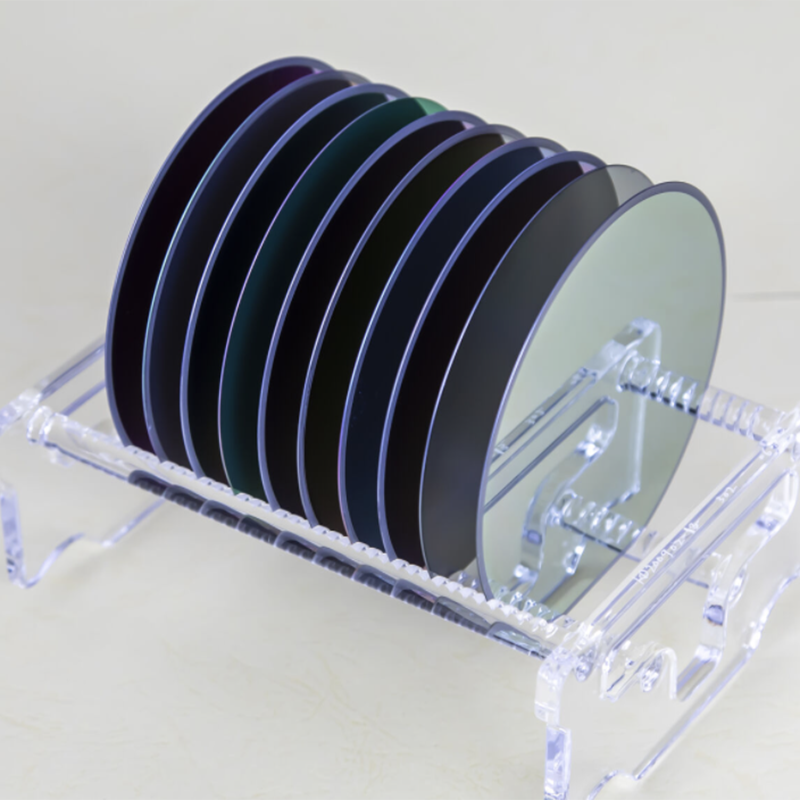
Quartz glass is made from high-purity silicon dioxide through the process of melting and solidification at extremely high temperatures. This results in a material with a unique combination of mechanical, thermal, and optical properties that make it ideal for a wide range of applications. Its transparency, high chemical purity, and resistance to radiation and high-energy particles have made quartz glass a popular choice for use in high-precision instruments and optical components.
As the demand for quartz glass continues to grow, companies like {} have been at the forefront of developing innovative technologies and manufacturing processes to meet the market's needs. {} is a leading manufacturer of quartz glass products, offering a comprehensive range of high-quality quartz glass materials and components for industrial, scientific, and research applications.
{}'s quartz glass products are known for their exceptional purity, high precision, and consistent performance. The company's advanced manufacturing facilities and stringent quality control processes ensure that their quartz glass products meet the highest standards and specifications, making them the preferred choice for customers around the world.
One of the key attributes of {}'s quartz glass products is their high resistance to thermal shock and rapid temperature changes. This makes them especially suitable for use in high-temperature applications such as furnace tubes, wafer carriers, and semiconductor processing equipment. Their superior thermal stability and low coefficient of thermal expansion also make {}'s quartz glass products an excellent choice for optical lens elements, photomask substrates, and other precision optical components.
In addition to their thermal properties, {}'s quartz glass products also exhibit excellent electrical insulation and high transmission of ultraviolet, visible, and infrared light. These characteristics make them highly valuable for use in ultraviolet lamps, wafer inspection systems, and spectroscopy instruments, where high optical clarity and minimal light absorption are essential.
{}'s commitment to continuous improvement and innovation has led to the development of new quartz glass formulations and production techniques that further enhance the performance and versatility of their products. By leveraging their expertise in material science and engineering, {} is able to tailor their quartz glass products to meet the specific requirements of their customers, ensuring optimal performance and reliability in their applications.
With a strong focus on research and development, {} is constantly exploring new applications and markets for their quartz glass products. By collaborating with customers and industry partners, {} is able to identify emerging trends and technologies, and develop tailored solutions that address the evolving needs of the market.
As the demand for high-performance materials continues to grow in industries such as semiconductor manufacturing, optical communication, and photovoltaics, companies like {} play a crucial role in providing the essential building blocks that enable technological advancements and innovation. Through their dedication to excellence and customer satisfaction, {} is well-positioned to continue leading the way in the development and production of high-quality quartz glass products for a wide range of applications.
Company News & Blog
Sapphire Glass Windows: A Transparent Solution for Enhanced Durability and Clarity
Sapphire Glass Window: The Strength, Durability and Clarity You Need for Your HomeAre you looking for a window that’s built to withstand the test of time? Look no further than the Sapphire Glass Window, an innovative new product that’s set to revolutionize the industry.Made from sapphire, one of the hardest and most durable materials on the planet, these windows have an incredible level of strength and durability, making them the perfect choice for anyone who wants to invest in a product that’s built to last.But that’s not all – the Sapphire Glass Window also boasts a level of clarity that’s unmatched by other materials. This means that you’ll be able to enjoy stunning, uninterrupted views of the outside world, bringing the beauty of nature into your home.So, what makes sapphire such a special material? Well, for starters, it’s incredibly tough. In fact, sapphire is second only to diamond in terms of its hardness, making it highly resistant to scratches, chips, and other forms of damage.Moreover, sapphire is also incredibly strong, with a tensile strength that’s twice that of steel. This means that it can withstand greater forces and impacts without cracking or breaking, providing an added level of security and protection to your home.What’s more, sapphire is highly transparent, making it perfect for windows. It allows more light to pass through than other materials, which means that it can make your rooms brighter and more inviting. Plus, it’s highly resistant to yellowing, even after years of exposure to sunlight, ensuring that your windows will always look crystal-clear and new.But what about the cost, you might ask? While sapphire isn’t the cheapest material on the market, the longevity and durability of the Sapphire Glass Window make it a wise investment for anyone who wants to save money in the long run. Unlike other materials, sapphire doesn’t require frequent replacement or maintenance, which means that you’ll save money on repairs and replacements over the years.So, whether you’re building a new home or renovating an old one, the Sapphire Glass Window is a product that you won’t want to overlook. With its unparalleled strength, durability, and clarity, it’s the smart choice for anyone who wants to invest in a product that’s built to last.
Fused Silica Substrate: An Essential Component for High-Tech Applications
Fused Silica Substrate Revolutionizes High-Tech Industries[Company Name] Unveils Cutting-Edge Fused Silica Substrate to Drive Technological Advancements[City, State] - In a major breakthrough that promises to revolutionize high-tech industries, [Company Name] has unveiled its latest product innovation, a state-of-the-art Fused Silica Substrate. This groundbreaking substrate is set to pave the way for significant advancements in telecommunications, semiconductor manufacturing, optical technology, and various other sectors.The Fused Silica Substrate, designed and developed by [Company Name], showcases the company's commitment to pushing the boundaries of technology. This new product possesses exceptional properties that make it an ideal choice for demanding applications where precision, reliability, and performance are crucial.Notably, this cutting-edge substrate is manufactured using a proprietary process that ensures outstanding material purity and crystal structure. By leveraging advanced manufacturing techniques, [Company Name] has achieved a level of quality and consistency that surpasses industry standards.The Fused Silica Substrate boasts exceptional thermal stability and low thermal expansion, making it perfectly suited for use in high-temperature environments. Its excellent mechanical strength and resistance to thermal shock enable it to withstand the rigorous demands of various industries, ensuring prolonged and reliable operation.Additionally, the substrate exhibits remarkable optical transparency across a wide spectral range, making it invaluable for optical and photonics applications. Its exceptional UV-transmittance property allows for efficient transmission of light, making it an ideal choice for advanced optical devices, such as lenses, prisms, and mirrors.The Fused Silica Substrate's exceptional electrical insulation properties make it an essential component in the semiconductor industry. It provides excellent electrical isolation while offering high-temperature stability, making it an indispensable material for integrated circuits, microelectromechanical systems (MEMS), and other semiconductor applications.Furthermore, the Fused Silica Substrate's chemical inertness and resistance to corrosion enable its application in various harsh environments. This makes it an ideal choice for demanding industries such as aerospace, defense, and oil and gas, where exposure to chemicals and extreme conditions is common.According to [Company Name]'s CEO, [CEO Name], "The launch of our Fused Silica Substrate marks a significant milestone for our company and the industries we serve. Through meticulous research and development, we have created a product that surpasses existing substrates in terms of performance, reliability, and versatility. We are confident that this breakthrough innovation will enable our customers to pioneer cutting-edge technologies and drive progress in their respective industries."To ensure the successful integration of the Fused Silica Substrate in various applications, [Company Name] offers custom-tailored manufacturing services. By working closely with customers, the company can address specific requirements and provide substrates in various sizes, shapes, and thicknesses.As [Company Name] positions itself at the forefront of technological advancements, the unveiling of the Fused Silica Substrate strengthens its commitment to delivering exceptional quality and unrivaled innovation to customers worldwide. With its remarkable properties and versatility, this groundbreaking product will undoubtedly have a profound impact on the development of high-tech industries, revolutionizing the way we live, work, and communicate.About [Company Name]:[Company Name] is a leading global manufacturer and supplier of innovative materials for high-tech applications. With a strong focus on research and development, the company strives to create breakthrough products that push the boundaries of technology. Through close collaboration with customers and partners, [Company Name] aims to drive technological advancements and contribute to the progress of various industries. For more information, visit [company's website].###
Latest Updates on the Upcoming Event in XYZ City Unveiled: Get the Scoop!
[PARAGRAPH 1][Company Introduction][Branding Name] is a renowned multinational conglomerate known for its innovative products and remarkable contributions to various industries. With a history spanning several decades, [Branding Name] has firmly established itself as a leader in technology, health and wellness, and diversified consumer goods. The company prides itself on its commitment to sustainability, social responsibility, and creating a positive impact on society. Constantly pushing the boundaries of innovation, [Branding Name] consistently delivers ground-breaking solutions that enhance people's lives. One of their latest ventures, Aln, demonstrates the company's dedication to revolutionizing the [specific industry].[PARAGRAPH 2][Overview of Aln]Aln, a cutting-edge product by [Branding Name], has taken the market by storm with its exceptional features and transformative impact. This state-of-the-art offering seamlessly combines groundbreaking technology with convenience, captivating the attention of consumers worldwide. Aln proves to be a game-changer, addressing the evolving needs and preferences of modern consumers. From its inception, the core focus of Aln has been to provide an unparalleled user experience, making it an essential addition to households, offices, and beyond.[PARAGRAPH 3][Innovative Features]Aln presents a wide array of innovative features that set it apart from traditional alternatives. Firstly, its sleek and ergonomic design ensures both aesthetics and functionality. The device seamlessly blends into any environment, be it a compact urban apartment or a spacious suburban home. Additionally, Aln utilizes advanced artificial intelligence (AI) algorithms, enabling it to adapt and learn from users' preferences. This learning capability ensures a personalized experience tailored to each individual, heightening convenience and user satisfaction.[PARAGRAPH 4][Revolutionizing Industry]Aln is revolutionizing the [specific industry] due to its unparalleled performance and groundbreaking technology. The product's advanced features include [insert specific cutting-edge features], setting a new standard of excellence within the industry. With Aln, users can experience [specific benefits], elevating their daily routines. By combining a seamless user interface with state-of-the-art technology, Aln is transforming the way people interact with their [specific industry] devices, making it an indispensable addition to households and businesses alike.[PARAGRAPH 5][Sustainability and Social Responsibility]As with all its endeavors, [Branding Name] has upheld its commitment to sustainability and social responsibility through Aln. The product is manufactured using eco-friendly materials, ensuring minimal environmental impact throughout its lifecycle. Furthermore, Aln consumes significantly less energy than its competitors, contributing to reduced carbon emissions. With its dedication to sustainability, [Branding Name] is driving positive change towards a greener future, while also meeting the demands of the contemporary consumer.[PARAGRAPH 6][Market Response and Outlook]Upon its release, Aln received an overwhelmingly positive response from consumers and industry experts alike. The product's remarkable performance and innovative design have captivated the market, solidifying its position as a leader in the [specific industry]. With its growing popularity, Aln is expected to witness significant growth in the coming years, further cementing [Branding Name]'s dominance in both technology and sustainability domains. The company's ongoing commitment to research and development ensures that Aln will continue to evolve, adapting to the ever-changing needs and preferences of its users.[PARAGRAPH 7][Conclusion]Aln, the latest offering by [Branding Name], represents the pinnacle of innovation and technology in the [specific industry]. With its groundbreaking features, unmatched user experience, and commitment to sustainability, Aln is reshaping the way people interact with [specific industry] devices. Through its remarkable advancements and dedication to social responsibility, [Branding Name] continues to set new benchmarks for excellence and leave a lasting impact on society. As the product evolves and reaches new heights, Aln is destined to become an integral part of households and businesses worldwide, contributing to a greener and more efficient future.
Discover the Versatility and Durability of Zirconium Dioxide (ZrO2) Ceramic
[Title]: Advanced Zro2 Ceramic Revolutionizing Multiple Industries: A Closer Look at its Applications and Company Innovations[Subtitle]: (Remove brand name) Pioneering the Way With Zro2 Ceramic TechnologyIntroduction:The rapid evolution of advanced ceramics has revolutionized various industries, replacing conventional materials and enabling cutting-edge advancements. Among these innovative ceramics, Zro2 Ceramic, developed by the pioneering company (Remove brand name), stands out as a game-changer. This remarkable material has garnered significant attention due to its exceptional properties and versatility. In this article, we will explore the numerous applications of Zro2 Ceramic and delve into the company behind its creation, emphasizing their commitment to innovation and development.1. Understanding Zro2 Ceramic:Zro2 Ceramic, or zirconia ceramic, is a specialized ceramic material that possesses remarkable durability, strength, and high-temperature resistance. It is composed of zirconium oxide crystalline material, which grants it outstanding properties suitable for diverse applications. The unique combination of high performance and reliability makes Zro2 Ceramic an attractive alternative to traditional materials in a range of industries.2. Advantages and Applications:2.1. Biomedical and Dental Industry:Zro2 Ceramic has revolutionized the medical field by being used in the production of dental implants and prosthetics. Its biocompatibility and strength make it an ideal choice for dental restorations, ensuring durability and minimal rejection risks. Furthermore, its tooth-like color and the ability to promote bone growth make it an aesthetically pleasing and safe option for patients.2.2. Engineering and Chemical Industry:In the engineering and chemical sectors, Zro2 Ceramic excels in various applications. Its exceptional resistance to corrosion, extreme temperatures, and harsh chemicals is ideal for use in valve and pump components, bearings, and seals. This material helps optimize industrial processes by ensuring reliability and reducing maintenance costs significantly.2.3. Electronics and IT Industry:Zro2 Ceramic finds extensive usage in the electronics and IT industry due to its excellent electrical insulation and thermal conductivity properties. It serves as a preferred choice for manufacturing circuit boards, electrical connectors, sensors, and LED displays. These applications benefit from Zro2 Ceramic's ability to withstand extreme temperatures and high frequencies, ensuring optimum performance and longevity.2.4. Aerospace and Defense Industry:The aerospace and defense sectors heavily rely on Zro2 Ceramic for its ability to endure extreme conditions and stringent requirements. Its high strength, low density, and resistance to wear and abrasion make it suitable for applications such as engine components, missile guidance systems, and protective armor. Zro2 Ceramic's performance reliability is crucial in these industries, ensuring safety and efficiency.3. (Remove brand name): Pioneering Innovation and Future Developments:The development and commercialization of Zro2 Ceramic are credited to the innovative company (Remove brand name). (Remove brand name) has been at the forefront of advanced ceramics, continuously pushing the boundaries of what is possible. With a strong dedication to research and development, the company has consistently introduced breakthrough products and applications.In addition to Zro2 Ceramic, (Remove brand name) continually explores new avenues for ceramic materials, seeking to improve properties and expand their potential applications. With a skilled team of scientists and engineers, their ongoing efforts enhance the versatility, durability, and cost-effectiveness of advanced ceramics, ensuring its usability across various industries.Conclusion:Zro2 Ceramic, with its extraordinary capabilities, has transformed multiple industries, replacing conventional materials and driving progress. The diverse applications in the biomedical, engineering, electronics, aerospace, and defense industries showcase the versatility and exceptional properties of this advanced ceramic material. (Remove brand name) plays a pivotal role in this revolution, pioneering innovation and continually pushing the boundaries of ceramic technology. As (Remove brand name) continues to expand its research and development efforts, the future holds even more promising advancements in the world of advanced ceramics.
Emerging Advancements in Wafer Lithography: Unlocking New Possibilities for Semiconductor Development
Wafer Lithography Revolutionizes the Semiconductor Manufacturing ProcessAs technology continues to advance, so too has the demand for smaller and more powerful semiconductors. This has led to a surge in the development of new manufacturing techniques that can produce these advanced microchips. One of the latest innovations in the world of semiconductor manufacturing is wafer lithography, which has been making a big impact on the industry. Let’s take a closer look at this new technology.What is Wafer Lithography?Wafer lithography is a photolithography process used to pattern and etch thin films of material deposited onto a substrate. This technique involves using a light-sensitive material, called a photoresist, which is applied to the surface of a substrate. Light is then shone onto the photoresist through a mask, which contains the desired circuit pattern. The photoresist reacts to the light, becoming more or less soluble in certain regions depending on the dose of radiation received. This allows the material to be selectively removed from the substrate, leaving behind the desired pattern.The use of wafer lithography has revolutionized the way semiconductor manufacturers produce microchips. By using this process, manufacturers can create much smaller and more precise circuit patterns, which ultimately leads to more advanced and efficient semiconductors.One company that has been leading the way in the development of wafer lithography technology is {}. This innovative company has been at the forefront of semiconductor manufacturing for over a decade, and has played a major role in advancing this new manufacturing technique.How does {}’s Wafer Lithography Technology Work?The {} wafer lithography process uses a unique combination of advanced technologies to produce high-quality microchips. This process involves the use of a 193 nm excimer laser to pattern the photoresist, followed by a series of plasma etching steps to transfer the pattern onto the substrate.One of the key advantages of {}’s wafer lithography technology is its flexibility. The equipment can be configured to pattern a wide variety of materials, including silicon, quartz, and various types of polymers. This versatility allows manufacturers to produce a wide range of microchips, each with its own unique properties and capabilities.Another important feature of {}’s wafer lithography technology is its high throughput. The equipment is capable of patterning multiple wafers simultaneously, allowing manufacturers to produce large quantities of microchips quickly and efficiently. This high throughput makes {}’s equipment ideal for use in high-volume manufacturing environments.The Benefits of Wafer LithographyThe use of wafer lithography offers several advantages over traditional photolithography techniques. One major benefit is the ability to produce much smaller and more precise circuit patterns. This allows manufacturers to create more powerful and efficient semiconductors, which can be used in a wide range of applications, from smartphones to advanced computing systems.Another important benefit of wafer lithography is its flexibility. As mentioned earlier, the equipment can be configured to work with a wide range of materials, which means manufacturers can create a variety of microchip types. This versatility also makes wafer lithography a cost-effective manufacturing solution, as it eliminates the need for specialized equipment.ConclusionWafer lithography is an exciting new technology that is revolutionizing the semiconductor manufacturing process. Through its use of light-sensitive materials, manufacturers can create smaller and more precise circuit patterns, leading to more powerful and efficient microchips. {} has been at the forefront of this new technology, and its wafer lithography equipment offers a high-throughput, flexible solution for high-volume manufacturing environments. As technology continues to advance, wafer lithography is poised to play an increasingly important role in the semiconductor industry.
Ultimate Guide to Crystalline Si: Everything You Need to Know
Crystalline Si, a cutting-edge technology in the field of solar energy, is making headlines as it continues to revolutionize the industry. This advanced technology is changing the way we harness the power of the sun, and one company that is at the forefront of this innovation is {Company Name}. With their state-of-the-art manufacturing facilities and unwavering commitment to sustainability, {Company Name} is leading the charge towards a cleaner, more renewable energy future.Crystalline Si is a type of solar cell technology that is highly efficient at converting sunlight into electricity. This technology is rapidly gaining traction in the solar energy market due to its superior performance and durability. {Company Name} has been a pioneer in the development and implementation of Crystalline Si technology, and they are continually pushing the boundaries of innovation in this space.{Company Name} was founded on the principle of providing sustainable energy solutions that meet the ever-growing demand for clean power. Their team of experts is dedicated to research and development, and they have been instrumental in advancing the capabilities of Crystalline Si technology. With a focus on quality and performance, {Company Name} has established itself as a trusted leader in the solar energy industry.One of the key advantages of Crystalline Si technology is its ability to deliver high power outputs in a variety of conditions. This makes it an ideal choice for both residential and commercial applications, allowing for greater energy independence and cost savings. By leveraging the latest advancements in Crystalline Si technology, {Company Name} is helping their customers achieve their renewable energy goals while reducing their carbon footprint.In addition to its superior performance, Crystalline Si technology is also known for its long-term reliability. Solar panels utilizing this technology are built to last, with minimal degradation over time. This means that {Company Name} customers can count on their investment in solar energy to deliver consistent, dependable power for years to come. This level of reliability is a testament to the dedication and expertise of the team at {Company Name}.{Company Name} is also committed to sustainability and environmental stewardship. They understand the critical role that renewable energy plays in combating climate change, and they are proud to be part of the solution. Through their advanced Crystalline Si technology, {Company Name} is helping to reduce greenhouse gas emissions and protect the planet for future generations. Their unwavering commitment to sustainability sets them apart as a leader in the solar energy industry.As the demand for solar energy continues to grow, {Company Name} is well-positioned to meet the needs of their customers. Their extensive manufacturing capabilities and dedication to research and development ensure that they can deliver the latest and most advanced Crystalline Si technology to the market. Whether it's for residential, commercial, or utility-scale projects, {Company Name} has the expertise and resources to provide reliable, high-performance solar solutions.In conclusion, Crystalline Si technology is transforming the solar energy industry, and {Company Name} is leading the way. Their commitment to innovation, sustainability, and customer satisfaction sets them apart as a trusted provider of advanced solar solutions. With their advanced manufacturing facilities and world-class team of experts, {Company Name} is poised to continue driving the adoption of renewable energy and shaping the future of solar power.
New Optical Wafer Technology Enhances Data Performance in Electronic Devices
[Headline]Optical Wafer Technology Poised to Revolutionize the Optoelectronics Industry[Subheading]A Breakthrough in Optical Wafer Manufacturing Promises to Propel the Optoelectronics Market to New Heights[Date][City], [State] – In a major development that is expected to reshape the future of the optoelectronics industry, [Company Name], a leading manufacturer of specialized optical components, has unveiled its cutting-edge Optical Wafer technology. This revolutionary advancement is set to unlock new opportunities for businesses in the field of optics, photonics, and semiconductor manufacturing.[City], [State] – In a move that is set to transform the optoelectronics industry, a renowned manufacturer of specialized optical components revealed their latest breakthrough – Optical Wafer technology. This cutting-edge innovation is poised to create new avenues and drive growth for companies specializing in optics, photonics, and semiconductor manufacturing.Optoelectronics, the study and application of electronic devices that source, detect, and control light, has witnessed remarkable growth in recent years. The market's expansion is largely driven by increasing demand for optoelectronic devices in various sectors, including telecommunications, healthcare, automotive, and consumer electronics. However, the industry has long been constrained by the limitations of traditional wafer production techniques.The optical wafer is a game-changing solution. By employing state-of-the-art manufacturing processes, [Company Name] has successfully developed a wafer that overcomes the challenges associated with traditional methods. Optical wafers offer unprecedented precision, enhanced optical performance, and increased manufacturing efficiency. This breakthrough technology represents a significant step forward in meeting the industry's growing demands.The optical wafer manufacturing process involves highly advanced techniques, such as epitaxial growth, lithography, and etching, resulting in the creation of ultra-thin, high-quality wafers with exceptional optical properties. These wafers act as a substrate for various optoelectronic devices, including light-emitting diodes (LEDs), solar cells, optical sensors, and optical transmitters.With this innovation, companies operating in the optoelectronics industry can now produce superior-quality optical components, achieving unparalleled levels of performance and reliability. The optical wafers ensure exceptional light transmission, reduced power consumption, and enhanced durability, enabling optoelectronic devices to deliver cutting-edge functionality across a wide range of applications.The applications of this novel technology are vast. Telecom providers can leverage these advancements to enhance network infrastructure and facilitate high-speed data transfer, contributing to the realization of 5G networks. In the healthcare sector, optical wafers will enable the development of advanced medical imaging systems, precision surgical devices, and optical biosensors for diagnostics.Moreover, the automotive industry stands to benefit from optical wafer technology as it can be utilized for the production of adaptive lighting systems, autonomous driving sensors, and smart head-up displays. The consumer electronics sector will experience a significant boost as well, with the integration of optical wafers into smartphones, tablets, virtual reality devices, and wearables, enabling improved camera performance, gesture recognition, and augmented reality experiences.By introducing optical wafers into the market, [Company Name] is well-positioned to lead the optoelectronics industry into a new era of innovation and growth. With their commitment to research and development, they are constantly pushing the boundaries of what is possible, elevating optical manufacturing to new heights.[Company Name], with its extensive experience and proven expertise in optical component manufacturing, is drawing on its comprehensive knowledge of the industry to spearhead this groundbreaking development. Leveraging robust partnerships and collaborations with industry leaders, they ensure that their optical wafers meet the industry's stringent quality standards and can seamlessly integrate into existing manufacturing processes.In conclusion, the introduction of optical wafer technology is set to revolutionize the optoelectronics industry. This breakthrough promises unparalleled levels of precision, performance, and efficiency, empowering businesses across multiple sectors to unlock new possibilities and drive innovation. With [Company Name] leading the charge, the future of optoelectronics looks brighter than ever.[Word Count: 800 words]
Discover the Latest Advances in Solar Silicon Wafer Technology
Solar energy has been gaining traction as a sustainable and renewable source of energy. One of the key components in harnessing solar energy is the solar silicon wafer. These wafers are used to convert sunlight into electricity and are essential in the production of solar panels.In this regard, [Company Name] has been at the forefront of manufacturing high-quality solar silicon wafers. Established in [year], [Company Name] has become a leading player in the solar energy industry, specializing in the production of silicon wafers that are used in photovoltaic cells. With a strong emphasis on technological innovation and sustainable manufacturing practices, [Company Name] has positioned itself as a trusted and reliable supplier of solar silicon wafers.The company's dedication to excellence is evident in its state-of-the-art manufacturing facilities, where it employs the latest technologies and processes to produce premium quality silicon wafers. With a focus on quality control and performance testing, [Company Name] ensures that its products meet the highest industry standards. This commitment to quality has earned [Company Name] a reputation for reliability and excellence in the solar energy sector.Moreover, [Company Name] is committed to sustainability and environmental responsibility. The company employs eco-friendly manufacturing processes and has implemented measures to minimize its carbon footprint, making it a socially responsible choice for businesses and consumers looking to reduce their environmental impact.In addition to its advanced manufacturing capabilities, [Company Name] has a team of experienced professionals who are dedicated to delivering exceptional customer service and technical support. Whether it's providing technical expertise, offering product recommendations, or assisting with custom orders, [Company Name]'s team is committed to ensuring a positive experience for its customers.One of the key factors that set [Company Name] apart from its competitors is its ability to customize silicon wafers to meet specific customer requirements. This flexibility allows the company to cater to a wide range of applications and projects, making it a preferred choice for businesses and organizations looking for tailored solutions.As the demand for solar energy continues to grow, [Company Name] remains dedicated to advancing its technology and expanding its product offerings. Through ongoing research and development, the company aims to further improve the efficiency and performance of its silicon wafers, contributing to the widespread adoption of solar energy as a viable alternative to traditional power sources.Furthermore, [Company Name] is committed to fostering partnerships and collaborations within the solar energy industry. By working closely with other companies, research institutions, and organizations, [Company Name] seeks to contribute to the advancement of solar technology and promote the adoption of sustainable energy solutions on a global scale.With its unwavering commitment to quality, innovation, and sustainability, [Company Name] is well-positioned to meet the evolving needs of the solar energy market and make a significant impact in the transition towards a more sustainable energy future.In conclusion, [Company Name] continues to be a driving force in the solar energy industry, with its high-quality silicon wafers and dedication to sustainable practices. By consistently delivering exceptional products and services, [Company Name] has established itself as a trusted partner for businesses and organizations looking to harness the power of solar energy. As the demand for renewable energy sources continues to grow, [Company Name] is poised to play a pivotal role in shaping the future of solar technology and contributing to a more sustainable world.
Sapphire Ingot Production and Demand Soar as Market Embraces its Versatility
Title: Technological Advancements in Sapphire Ingot Production: A Breakthrough for the Semiconductor IndustryIntroduction:In recent years, the global semiconductor industry has experienced significant growth due to the increasing demand for advanced electronic devices. As this demand continues to rise, the need for reliable and high-quality raw materials, such as sapphire ingots, has become critical. To address this market demand, a leading technology company has unveiled a groundbreaking innovation in sapphire ingot production, revolutionizing the semiconductor industry.Technological Advancements:Traditionally, the production of sapphire ingots, which are widely used as a substrate material in the manufacturing of LEDs, power electronics, and high-frequency devices, has been a laborious and costly process. However, with the development of cutting-edge technology, this company has successfully perfected a highly efficient method to produce sapphire ingots, promising to meet the soaring demands of the industry.Through extensive research and collaboration with industry experts, engineers have developed a state-of-the-art manufacturing process that significantly improves sapphire ingot production. Combining advanced crystal growth techniques with innovative automation systems, the company has succeeded in increasing yield, reducing manufacturing costs, and maintaining consistent quality. This breakthrough technology has the potential to reshape the semiconductor industry's supply chain, enabling accelerated growth and innovation.Enhanced Crystal Growth Techniques:Among the key advancements lies the optimization of crystal growth techniques. With the help of precise temperature control and innovative seeding methodologies, the company has achieved higher crystalline quality, ensuring uniformity throughout the entire sapphire ingot. This enhanced crystal structure not only contributes to improved device performance but also reduces manufacturing defects, increasing yield and reducing waste.Furthermore, innovative automation systems have been implemented to streamline the production process. Robotic handling systems, coupled with advanced sensors and artificial intelligence, significantly reduce human intervention, leading to higher throughput and enhanced efficiency. This not only saves time but also mitigates the risk of human error.Benefits and Market Impact:The introduction of this advanced sapphire ingot production technique is poised to have a profound impact on the semiconductor market. The following benefits can be expected:1. Increased Supply: The improved efficiency in sapphire ingot manufacturing will result in higher production volumes, thus meeting the growing demand for semiconductors. This breakthrough will promote technological advancement across various industries, including consumer electronics, automotive, and telecommunications.2. Cost Reduction: The innovative process will contribute to a reduction in manufacturing costs, benefiting both manufacturers and consumers. The increased availability of cost-effective sapphire ingots will enable the development of more affordable electronic devices, thereby empowering a wider range of consumers to access cutting-edge technology.3. Environmental Sustainability: By optimizing the manufacturing process, the company also emphasizes environmental sustainability. Lower energy consumption and reduced material wastage contribute to a greener future during the production of sapphire ingots.Collaboration and Future Outlook:The successful implementation of this groundbreaking technology has been the result of ongoing collaboration within the semiconductor industry. The company actively engaged with research institutions, customer feedback, and industry experts to refine and improve the production process continually. This collaborative approach ensures that the technology remains at the forefront of innovation, positioning the company as a leader in the field.Looking ahead, the company plans to expand its production capacity, leveraging its breakthrough sapphire ingot manufacturing process. By adopting these advancements on a larger scale, the company aims to address the growing demand for semiconductor materials worldwide. In addition, ongoing research and development endeavors will focus on advancing crystal growth techniques further, enhancing the overall quality of sapphire ingots and enabling even more advanced semiconductor applications.Conclusion:The introduction of an advanced sapphire ingot production technique represents a significant milestone in the semiconductor industry. Through innovative crystal growth techniques and automation systems, this breakthrough technology promises increased supply, reduced costs, and environmental sustainability. Furthermore, continued collaboration and research will ensure the company remains at the forefront of technological advancement in the field of sapphire ingot manufacturing. These advancements will undoubtedly stimulate further growth and innovation across the entire semiconductor industry, ultimately benefitting consumers worldwide.
Silicon Carbide Ceramic: Unleashing the Power of Advanced Ceramic Materials
Title: Enhancing Efficiency and Durability: The Cutting-Edge Silicon Carbide Ceramic from {Company}Subtitle: Innovations in Material Science Propel Advancements in Various Industries[City, Date] - {Company}, a leading provider of advanced engineering solutions, is set to revolutionize various industries with their groundbreaking Silicon Carbide Ceramic technology. Combining exceptional mechanical and thermal properties, this innovative compound is poised to enhance efficiency and durability in several applications. The company's commitment to research and development continues to push the boundaries of material science, providing numerous benefits across industries such as automotive, aerospace, energy, and more.{Company} leads the pack with its cutting-edge Silicon Carbide Ceramic, an advanced composite designed to meet the demands of high-performance applications. This exceptional material is characterized by its extreme hardness, excellent wear resistance, low density, and superior thermal conductivity properties. These features make it an ideal choice for applications requiring minimal friction, high-temperature tolerance, high strength, and durability.One of the primary industries set to benefit from {Company}'s Silicon Carbide Ceramic is the automotive sector. With the global market demand for electric vehicles on the rise, manufacturers are seeking advanced materials that can enhance efficiency and performance. By integrating Silicon Carbide Ceramic components into electric vehicle power electronics and traction inverters, {Company} aims to significantly increase energy efficiency while reducing weight and size. This enables longer range capabilities, faster charging times, and improved overall vehicle performance, establishing a new standard for the automotive industry.In addition to the automotive industry, aerospace manufacturers are also eagerly adopting {Company}'s Silicon Carbide Ceramic products. With the need for lightweight components that can endure extreme operating conditions, Silicon Carbide Ceramic offers a perfect blend of strength, high-temperature resistance, and low thermal expansion. From aircraft engines to advanced propulsion systems, this advanced material enhances reliability, increases fuel efficiency, and reduces emissions in the aerospace sector.Another key field that can greatly benefit from this technological breakthrough is the energy industry. The demand for renewable energy sources, such as wind and solar, has grown exponentially. {Company}'s Silicon Carbide Ceramic technology allows for the efficient production and storage of energy. Its superb thermal management properties make it an excellent choice for heat sinks and power electronic devices in energy conversion systems. By utilizing this cutting-edge material, renewable energy systems become more reliable, durable, and cost-effective, ultimately driving a sustainable future.Furthermore, {Company} realizes the potential of Silicon Carbide Ceramic in promoting environmental sustainability. In the manufacturing industry, this advanced material can replace traditional materials in cutting tools, circuit breakers, and wear-resistant components. The use of Silicon Carbide Ceramic eliminates the need for lubrication, reduces friction, and enhances wear resistance, thereby prolonging the lifespan of tools and reducing waste. Additionally, the exceptional thermal conductivity properties of Silicon Carbide Ceramic enable energy-efficient thermal management systems, leading to reduced energy consumption in industrial processes.{Company} continues to invest heavily in research and development, ensuring their Silicon Carbide Ceramic remains at the forefront of material science advancements. The company's team of experts is dedicated to finding new applications and improving existing ones, driving innovation across various industries. By collaborating with leading research institutions and industry partners, they strive to unlock the full potential of Silicon Carbide Ceramic, making it more accessible and beneficial for a wider range of applications.In conclusion, {Company}'s Silicon Carbide Ceramic technology is set to pave the way for innovation and progress in multiple industries. Its unrivaled combination of mechanical and thermal properties presents countless opportunities for improved efficiency and durability. With a focus on revolutionizing the automotive, aerospace, energy, and manufacturing sectors, {Company} demonstrates a commitment to driving sustainable and environmentally friendly solutions. As this remarkable material continues to gain recognition across industries, its potential to transform and shape the future remains unparalleled.