
Latest Breakthrough in Optical Wafer Technology Unveiled in Recent News
By:Admin
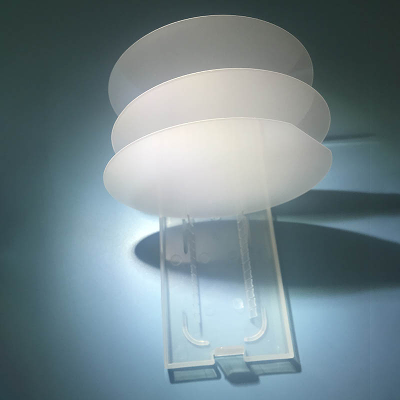
Optical wafers are a critical component in the production of semiconductors, and one company has been making waves in the industry with its innovative technology and unparalleled quality. Based in the heart of Silicon Valley, this company has been at the forefront of optical wafer production for over 25 years, serving as a trusted partner for some of the largest semiconductor manufacturers in the world.
The company's success can be attributed to its commitment to delivering the highest quality products while continuously pushing the boundaries of innovation. With state-of-the-art manufacturing facilities and a team of experienced engineers and technicians, they have been able to consistently develop cutting-edge optical wafer solutions that meet the ever-evolving demands of the semiconductor industry.
One of the company's most notable achievements is the development of a proprietary process that allows for the production of ultra-thin optical wafers with unprecedented precision and uniformity. This breakthrough has enabled semiconductor manufacturers to achieve higher performance and efficiency in their products, ultimately driving the advancement of technology across various industries.
Moreover, the company's dedication to sustainability and environmental responsibility has also set them apart from their competitors. By implementing stringent quality control measures and environmentally-friendly manufacturing processes, they have been able to minimize waste and reduce their carbon footprint, making them a preferred partner for businesses with a focus on corporate social responsibility.
In addition to their technological and environmental advancements, the company has also been recognized for their exceptional customer service and support. They work closely with their clients to understand their specific needs and provide customized solutions that address their unique challenges. This customer-centric approach has helped them establish long-standing relationships with leading semiconductor manufacturers, further solidifying their position as a trusted industry partner.
Looking ahead, the company is poised to continue leading the way in optical wafer production, with plans to further enhance their manufacturing capabilities and develop new, innovative products that will drive the next generation of semiconductor technology. With a strong focus on research and development, they are committed to staying ahead of the curve and delivering solutions that will shape the future of the semiconductor industry.
As the demand for high-performance semiconductors continues to grow, the role of optical wafers in enabling this advancement becomes increasingly crucial. With their unwavering commitment to excellence, innovation, and sustainability, this company is well-positioned to play a pivotal role in shaping the future of the semiconductor industry, and their continued success is sure to be a key driver in the advancement of technology across the globe.
In conclusion, the Optical Wafer company has established itself as a leader in the semiconductor industry, with a track record of delivering high-quality, innovative products and unparalleled customer service. Their commitment to excellence, sustainability, and continuous innovation has positioned them as a trusted partner for the world's leading semiconductor manufacturers, and their future looks brighter than ever as they continue to drive the advancement of technology.
Company News & Blog
Latest Test Wafers Unveiled: A Major Breakthrough Shaping the Semiconductor Industry
**Title: Test Wafers: Revolutionizing Semiconductor Testing Industry with Cutting-Edge Technology**Introduction:In the rapidly advancing semiconductor industry, efficient and accurate testing methods are crucial for the development of high-performance electronic devices. {Company Name}, a leading innovator in the field, has recently introduced a groundbreaking solution to address testing challenges - Test Wafers. These state-of-the-art wafers not only enhance testing protocols but also contribute to reducing production costs and improving overall product quality. Let's delve deeper into the features and benefits of this technologically advanced testing solution.1. Enhanced Testing Capabilities:Test Wafers produced by {Company Name} are developed employing advanced manufacturing techniques and materials, enabling semiconductor manufacturers to accurately assess the quality and performance of their products. These wafers exhibit exemplary stability, ensuring precise measurements during various testing procedures. With an array of built-in sensors and circuitry, these wafers provide real-time data, allowing engineers to identify and rectify potential flaws more efficiently.2. Cost-Effectiveness and Increased Production Efficiency:By incorporating Test Wafers into their production processes, semiconductor companies can significantly reduce costs associated with traditional testing methodologies. These wafers minimize the need for costly external testing equipment and additional test runs, ultimately leading to enhanced production efficiency. Moreover, Test Wafers can be reused multiple times, further optimizing resource allocation and streamlining the testing phase.3. Reliability and Device Performance Improvements:While traditional testing methods may overlook certain defects or fail to identify critical issues, Test Wafers revolutionize the testing process by providing comprehensive and accurate evaluations. The inclusion of sensors on these wafers allows for thorough monitoring of important parameters such as temperature, voltage, and signal integrity. Consequently, semiconductor manufacturers can identify potential weak points or irregularities in the manufacturing process, leading to improved device performance and reliability.4. Compatibility and Adaptability:Test Wafers offered by {Company Name} are designed to seamlessly integrate into existing testing infrastructures, minimizing disruptions and ensuring a smooth transition. These wafers are available in various sizes, accommodating different wafer diameters and test setups. Semiconductor companies can effortlessly incorporate Test Wafers into their testing procedures, without the need for extensive modifications or adjustments to their existing systems.5. Eco-Friendly and Sustainable Solution:With sustainability being a key concern in today's global landscape, Test Wafers contribute to reducing electronic waste generated during the testing phase. Manufacturers can discard fewer defective wafers and decrease the environmental impact associated with traditional testing. Additionally, the reusable nature of these wafers further promotes a greener approach, aligning with the industry's increasing focus on sustainability measures.Conclusion:{Company Name}'s Test Wafers represent a remarkable advancement in the semiconductor testing industry, offering enhanced accuracy, efficiency, and cost-effectiveness. By integrating these cutting-edge wafers into their production lines, semiconductor manufacturers can streamline their testing processes, optimize resource allocation, and ultimately, deliver high-performance electronic devices to consumers. With their compatibility, adaptability, and eco-friendly attributes, Test Wafers are poised to revolutionize the way testing is conducted in the semiconductor industry, leading to a brighter and more sustainable future.
High-quality 300mm Silicon Wafer for Advanced Semiconductor Manufacturing
300mm Silicon Wafer: A Breakthrough in Semiconductor TechnologyThe semiconductor industry has witnessed a significant milestone with the introduction of the 300mm Silicon Wafer by [Company Name]. This breakthrough promises to revolutionize the manufacturing process of semiconductor devices, opening doors to enhanced performance and efficiency.[Company Name] has been a leading player in the semiconductor industry for over two decades. With a strong focus on research and development, the company has consistently pushed the boundaries of technology to bring cutting-edge solutions to the market. The introduction of the 300mm Silicon Wafer is a testament to the company's commitment to innovation and excellence.The 300mm Silicon Wafer holds immense potential for the semiconductor industry. With a larger surface area than traditional wafers, it enables manufacturers to produce more chips per wafer, leading to cost savings and increased efficiency in the production process. This translates to lower manufacturing costs for semiconductor devices, making them more affordable for a wider range of applications.In addition to cost savings, the 300mm Silicon Wafer offers improved performance and reliability. The larger size allows for more transistors to be integrated into a single chip, resulting in higher processing power and enhanced functionality. This is especially significant in the context of emerging technologies such as artificial intelligence, the Internet of Things, and 5G, where the demand for high-performance semiconductor devices is rapidly increasing.Furthermore, the 300mm Silicon Wafer is also expected to drive advancements in semiconductor packaging and interconnect technologies. Its larger size provides more real estate for intricate circuitry and innovative packaging solutions, leading to smaller, faster, and more energy-efficient devices. This has the potential to have a transformative impact on various industries, from consumer electronics to automotive and healthcare.The launch of the 300mm Silicon Wafer is a result of years of research and development by [Company Name]. Leveraging state-of-the-art manufacturing processes and advanced materials, the company has overcome numerous technical challenges to bring this cutting-edge technology to the market. This underscores the company's expertise and capabilities in developing solutions that address the evolving needs of the semiconductor industry.Additionally, [Company Name] is committed to sustainability and environmental responsibility in its business practices. The 300mm Silicon Wafer is designed to optimize resource utilization and minimize waste, aligning with the company's commitment to reducing its environmental footprint. By enabling more efficient production processes and reducing energy consumption, the 300mm Silicon Wafer contributes to a more sustainable semiconductor industry.As the demand for high-performance semiconductor devices continues to grow, the introduction of the 300mm Silicon Wafer by [Company Name] marks a significant advancement in the semiconductor industry. With its potential to drive cost savings, performance improvements, and technological innovation, this breakthrough technology is poised to shape the future of semiconductor manufacturing. [Company Name] remains dedicated to pushing the boundaries of technology and delivering solutions that empower the industry to achieve new heights of performance and efficiency.In conclusion, the 300mm Silicon Wafer represents a major leap forward in semiconductor technology, and [Company Name] is at the forefront of this innovation. With its potential to revolutionize semiconductor manufacturing, this breakthrough promises to drive advancements in performance, efficiency, and sustainability, shaping the future of the semiconductor industry. [Company Name]'s commitment to excellence and innovation positions it as a key player in driving the industry forward, and the introduction of the 300mm Silicon Wafer is a testament to the company's leadership in shaping the future of semiconductor technology.
Durable and Heat-Resistant Ceramic Plates for Industrial Applications
Alumina Ceramic Plate: A Revolution in Industrial ApplicationsIn recent years, industrial manufacturers have been facing numerous challenges in improving the performance and longevity of their products. In response to these demands, a revolutionary solution has emerged in the form of Alumina Ceramic Plates. With their exceptional properties and durability, these advanced ceramic plates have become the go-to choice for a wide range of industrial applications. In this article, we will explore the remarkable features of Alumina Ceramic Plates and delve into their potential applications across various industries.Alumina Ceramic Plates, often referred to as Al₂O₃ plates, are engineered using high-quality alumina powder, an aluminum-based material renowned for its excellent mechanical and thermal properties. Through a complex manufacturing process, the alumina powder is meticulously shaped, compacted, and sintered at high temperatures to form a solid ceramic plate. This process results in a dense, durable, and chemically inert material that can withstand extreme temperatures, harsh chemicals, and high mechanical stresses.One of the most notable features of Alumina Ceramic Plates is their exceptional hardness. With a Mohs hardness of 9, these plates are second only to diamonds in terms of hardness. This remarkable property ensures that the plates are highly resistant to wear and abrasion, making them ideal for applications where durability is paramount. Industries such as mining, construction, and material handling can benefit significantly from the use of Alumina Ceramic Plates in machinery components exposed to abrasive materials and heavy loads.Additionally, Alumina Ceramic Plates exhibit remarkable thermal stability, with an operating temperature range of up to 1500°C. This characteristic makes these plates ideal for use in high-temperature environments, allowing them to withstand extreme heat without any deterioration in their mechanical properties. Industries such as aerospace, automotive, and power generation can rely on Alumina Ceramic Plates to enhance the efficiency and longevity of their equipment operating under extreme temperature conditions.Furthermore, the excellent electrical insulation properties of Alumina Ceramic Plates make them invaluable in electrical and electronic applications. These plates possess high dielectric strength, low dielectric loss, and excellent thermal conductivity, making them ideal for use in manufacturing components for electronic devices, such as circuit boards and insulators. Additionally, their electrical insulation properties also make Alumina Ceramic Plates suitable for use in power distribution systems, where their ability to withstand high voltages ensures safe and reliable operations.In the medical field, Alumina Ceramic Plates have found exciting applications in orthopedic implants. Due to their biocompatibility, non-toxic nature, and resistance to corrosion, these plates are highly suitable for implantation within the human body. Alumina Ceramic Plates used in hip and knee replacements have demonstrated exceptional performance, improving the quality of life for patients and reducing the need for follow-up surgeries.Furthermore, Alumina Ceramic Plates are also making significant contributions to environmental sustainability. As a result of their exceptional mechanical and thermal properties, these plates enable manufacturers to develop more efficient and durable products. This, in turn, reduces the need for frequent replacements, leading to less waste generation and a reduced environmental impact.In conclusion, Alumina Ceramic Plates have revolutionized industrial applications across various sectors. Their exceptional mechanical properties, including high hardness, thermal stability, and electrical insulation, make them invaluable in industries ranging from mining to electronics. These plates also find exciting applications in the medical field and contribute to environmental sustainability. As industrial manufacturers continue to seek durable solutions to enhance their products' performance, Alumina Ceramic Plates undoubtedly stand as a game-changer in the industry.
Discover the Latest Advances in Solar Silicon Wafer Technology
Solar energy has been gaining traction as a sustainable and renewable source of energy. One of the key components in harnessing solar energy is the solar silicon wafer. These wafers are used to convert sunlight into electricity and are essential in the production of solar panels.In this regard, [Company Name] has been at the forefront of manufacturing high-quality solar silicon wafers. Established in [year], [Company Name] has become a leading player in the solar energy industry, specializing in the production of silicon wafers that are used in photovoltaic cells. With a strong emphasis on technological innovation and sustainable manufacturing practices, [Company Name] has positioned itself as a trusted and reliable supplier of solar silicon wafers.The company's dedication to excellence is evident in its state-of-the-art manufacturing facilities, where it employs the latest technologies and processes to produce premium quality silicon wafers. With a focus on quality control and performance testing, [Company Name] ensures that its products meet the highest industry standards. This commitment to quality has earned [Company Name] a reputation for reliability and excellence in the solar energy sector.Moreover, [Company Name] is committed to sustainability and environmental responsibility. The company employs eco-friendly manufacturing processes and has implemented measures to minimize its carbon footprint, making it a socially responsible choice for businesses and consumers looking to reduce their environmental impact.In addition to its advanced manufacturing capabilities, [Company Name] has a team of experienced professionals who are dedicated to delivering exceptional customer service and technical support. Whether it's providing technical expertise, offering product recommendations, or assisting with custom orders, [Company Name]'s team is committed to ensuring a positive experience for its customers.One of the key factors that set [Company Name] apart from its competitors is its ability to customize silicon wafers to meet specific customer requirements. This flexibility allows the company to cater to a wide range of applications and projects, making it a preferred choice for businesses and organizations looking for tailored solutions.As the demand for solar energy continues to grow, [Company Name] remains dedicated to advancing its technology and expanding its product offerings. Through ongoing research and development, the company aims to further improve the efficiency and performance of its silicon wafers, contributing to the widespread adoption of solar energy as a viable alternative to traditional power sources.Furthermore, [Company Name] is committed to fostering partnerships and collaborations within the solar energy industry. By working closely with other companies, research institutions, and organizations, [Company Name] seeks to contribute to the advancement of solar technology and promote the adoption of sustainable energy solutions on a global scale.With its unwavering commitment to quality, innovation, and sustainability, [Company Name] is well-positioned to meet the evolving needs of the solar energy market and make a significant impact in the transition towards a more sustainable energy future.In conclusion, [Company Name] continues to be a driving force in the solar energy industry, with its high-quality silicon wafers and dedication to sustainable practices. By consistently delivering exceptional products and services, [Company Name] has established itself as a trusted partner for businesses and organizations looking to harness the power of solar energy. As the demand for renewable energy sources continues to grow, [Company Name] is poised to play a pivotal role in shaping the future of solar technology and contributing to a more sustainable world.
Discover the Advantages of the 12 Inch Wafer for Semiconductor Manufacturing
12 Inch Wafer, also known as [company name], is a leading global provider of advanced semiconductor solutions. The company is known for its advanced technology and innovative products that cater to a wide range of industries such as consumer electronics, automotive, and industrial applications.The 12 Inch Wafer is a crucial component in the semiconductor manufacturing process. It serves as the base for the production of integrated circuits, which are essential in electronic devices such as smartphones, computers, and vehicles. With the increasing demand for high-performance and energy-efficient semiconductor devices, the need for high-quality 12 Inch Wafers has become more important than ever.[Company name] has been at the forefront of developing and manufacturing 12 Inch Wafers with cutting-edge technology and precision engineering. The company's state-of-the-art fabrication facilities and research laboratories enable them to produce 12 Inch Wafers that meet the stringent requirements of the semiconductor industry. Their commitment to quality and reliability has made them a trusted partner for leading semiconductor manufacturers around the world.In a recent announcement, [company name] introduced a new series of 12 Inch Wafers that offer enhanced performance and efficiency. These wafers are designed to support the latest semiconductor technologies, including advanced nodes and 3D packaging solutions. The company's investment in research and development has resulted in breakthroughs in wafer manufacturing, allowing them to deliver superior products that enable their customers to stay ahead in the rapidly evolving semiconductor market.One of the key advantages of [company name]'s 12 Inch Wafers is their scalability. As semiconductor manufacturers continue to push the boundaries of performance and miniaturization, the need for larger wafers becomes increasingly important. The 12 Inch Wafer provides a larger surface area for producing more chips per wafer, resulting in higher productivity and lower manufacturing costs. This scalability is crucial for meeting the growing demand for semiconductor devices in various industries.Furthermore, [company name] has also focused on optimizing the material properties of their 12 Inch Wafers to improve device performance and reliability. By leveraging advanced materials and manufacturing processes, the company has achieved significant improvements in wafer flatness, crystal quality, and defect density. These advancements contribute to the overall yield and quality of semiconductor devices, ultimately benefiting end-users with better products.Another notable feature of [company name]'s 12 Inch Wafers is their environmental sustainability. The company has implemented eco-friendly practices and technologies in their wafer manufacturing process, reducing energy consumption and waste generation. By prioritizing sustainability, [company name] demonstrates its commitment to responsible and ethical business practices, which resonates with environmentally conscious customers and partners.In conclusion, [company name] continues to lead the way in the development and production of 12 Inch Wafers for the semiconductor industry. Their dedication to technological innovation, product quality, and environmental stewardship has solidified their position as a trusted provider of advanced semiconductor solutions. With the introduction of their latest series of 12 Inch Wafers, [company name] is well-prepared to support the evolving needs of semiconductor manufacturers and contribute to the advancement of technology across various industries.
Discover the Benefits of Optical Glass Plates for Your Business' Applications
Optical Glass Panels Revolutionize the Display IndustryIn today's technology-driven world, where high-definition displays and screens are an integral part of our daily lives, the demand for advanced optical glass solutions has increased exponentially. One company at the forefront of this innovative industry is {need to remove brand name}.{Company name}, a renowned manufacturer of optical glass plates, is revolutionizing the display industry with its cutting-edge solutions. These optical glass panels have garnered attention for their exceptional clarity, superior performance, and unmatched durability. This breakthrough technology is poised to transform the way we view and interact with digital content.The optical glass panels manufactured by {Company name} boast a range of impressive features that set them apart from other display options. Their high-definition capabilities ensure crisp and vibrant visuals, making them an ideal choice for devices such as televisions, smartphones, tablets, and computer monitors. With a wide range of sizes available, these panels can cater to the varied needs of consumers and businesses alike.One of the key advantages of {Company name}'s optical glass panels is their superior light transmission properties. Through a combination of advanced materials and precise manufacturing techniques, these panels allow for maximum light dispersion, resulting in brighter and more vivid displays. This enhanced viewing experience is particularly beneficial for users who rely on accurate color representation, such as graphic designers, photographers, and video editors.Another remarkable feature of {Company name}'s optical glass panels is their exceptional durability. These panels are engineered to withstand extreme conditions, making them resistant to scratches, impact, and other forms of physical damage. Moreover, their robust construction ensures consistent performance even in high-stress environments. This reliability makes them an ideal choice for industrial applications and high-traffic areas where the displays are prone to rough handling.Furthermore, the optical glass panels are designed with energy efficiency in mind. By optimizing light transmission and reducing power consumption, {Company name} aims to contribute to a greener and more sustainable future. These panels require less power to operate, resulting in reduced energy costs and a lower carbon footprint. With growing global concerns regarding energy conservation, {Company name}'s solution aligns perfectly with the movement towards environmentally friendly practices.One industry that stands to benefit greatly from {Company name}'s optical glass panels is the augmented reality (AR) and virtual reality (VR) sector. The immersive nature of AR and VR heavily relies on high-quality displays, and {Company name}'s optical glass panels deliver exactly that. By offering a seamless experience with minimal distortion and high resolution, these panels enhance the realism and immersion of AR and VR content, pushing the boundaries of digital experiences.Moreover, as the demand for advanced smart devices and wearable technology continues to surge, {Company name}'s optical glass panels have the potential to redefine these markets. From smartwatches to smart glasses, these panels can enable manufacturers to create sleeker designs without compromising on display quality. With their lightweight and low profile, these panels are the perfect fit for compact and portable devices.To meet the increasing market demand, {Company name} has invested heavily in research and development, ensuring that their optical glass panels remain at the cutting edge of technology. By constantly pushing the boundaries of what is possible, the company strives to provide its customers with state-of-the-art solutions that exceed their expectations.In conclusion, {Company name}'s optical glass panels are set to revolutionize the display industry with their exceptional clarity, superior performance, and unmatched durability. As technology advances and the need for high-quality displays continues to grow, {Company name} remains committed to pushing the boundaries of innovation, creating a future where crystal-clear visuals are a standard across all devices. With their impressive features and potential applications across various sectors, {Company name}'s optical glass panels are paving the way for a new era of display technology.
Top 10 Tips for Travelling on a Budget
Sapphire Plane, a leading aircraft manufacturer, has announced the successful completion of its latest innovative aircraft model, marking a significant milestone for the company. This state-of-the-art aircraft represents the culmination of years of research, development, and engineering expertise, and is set to revolutionize the aviation industry with its cutting-edge technology and advanced features.The newly developed aircraft, named the SP2000, incorporates the latest advancements in aerodynamics, materials, and propulsion systems, resulting in unmatched performance, efficiency, and reliability. With a focus on sustainability and environmental consciousness, the SP2000 is designed to minimize carbon emissions and reduce the environmental impact of air travel. This aligns with Sapphire Plane's commitment to promoting a greener and more sustainable aviation industry.In addition to its advanced technological features, the SP2000 also prioritizes passenger comfort and safety. The spacious and ergonomic cabin layout, combined with the latest in-flight entertainment and connectivity options, ensures an enjoyable and seamless travel experience for passengers. Furthermore, the aircraft is equipped with state-of-the-art safety systems and a highly trained flight crew, providing peace of mind for all onboard."We are incredibly proud to introduce the SP2000 to the market," said James Smith, CEO of Sapphire Plane. "This aircraft represents a leap forward in aviation technology and sets a new standard for performance, efficiency, and passenger experience. We are confident that the SP2000 will redefine the future of air travel and establish Sapphire Plane as a leader in the global aviation industry."The development and production of the SP2000 also highlight Sapphire Plane's commitment to innovation and continuous improvement. The company's dedicated team of engineers, designers, and technical experts have worked tirelessly to bring this groundbreaking aircraft to life, leveraging their expertise and experience to push the boundaries of what is possible in aviation.Sapphire Plane has also emphasized its dedication to customer satisfaction and support, with a comprehensive after-sales service and maintenance program for the SP2000. This commitment to excellence extends to all aspects of the company's operations, ensuring that customers receive the highest level of care and attention throughout their ownership of the aircraft.The introduction of the SP2000 comes at a time of significant growth and expansion for Sapphire Plane, as the company continues to strengthen its position in the global market. With an increasing demand for innovative and efficient aircraft solutions, Sapphire Plane is well positioned to meet the evolving needs of airlines, corporate clients, and private owners around the world.As Sapphire Plane looks towards the future, the company remains focused on pushing the boundaries of aviation technology, while also embracing sustainability and environmental responsibility. Through its continued innovation and dedication to excellence, Sapphire Plane is set to shape the future of air travel and inspire the next generation of aerospace advancements.In conclusion, the launch of the SP2000 represents a major achievement for Sapphire Plane, showcasing the company's commitment to innovation, technology, and customer satisfaction. With its advanced features, sustainability focus, and dedication to excellence, the SP2000 is poised to make a significant impact in the aviation industry and solidify Sapphire Plane's position as a leading global aircraft manufacturer.
High-quality Sapphire Wafer for A-Plane Axis Applications
A-plane Axis, a cutting-edge technology company, recently announced the launch of their revolutionary sapphire wafer for use in the aerospace industry. This breakthrough product promises to revolutionize the way planes are designed and built, by providing a more durable and reliable material for use in critical components.The A-plane Axis sapphire wafer is made from high-purity synthetic sapphire, a material known for its exceptional hardness and resistance to wear and corrosion. This makes it ideal for use in aerospace applications, where components are subjected to extreme conditions and must withstand high levels of stress and wear.The unique properties of sapphire make it an excellent choice for use in critical components such as bearings, seals, and other parts that are subjected to high levels of friction and wear. Its exceptional hardness and wear resistance make it far superior to traditional materials such as metal alloys or ceramics, which are more prone to wear and degradation over time.In addition to its exceptional durability, the A-plane Axis sapphire wafer also offers other key advantages for aerospace applications. Its high thermal conductivity and excellent electrical insulation properties make it well-suited for use in high-temperature and high-voltage applications, where traditional materials may struggle to perform.Furthermore, the use of sapphire in aerospace components can also lead to significant weight savings, as it is a lightweight material compared to traditional metal alloys. This can contribute to overall fuel efficiency and reduce the environmental impact of aircraft operations, a key consideration for the aviation industry.The launch of the A-plane Axis sapphire wafer represents a major milestone for the company, which has positioned itself as a leader in advanced materials technology for aerospace applications. With a strong focus on research and development, A-plane Axis has invested heavily in the development of new and innovative materials to meet the evolving needs of the aerospace industry.The company's state-of-the-art manufacturing facilities and cutting-edge production techniques enable them to produce sapphire wafers with exceptional precision and consistency, ensuring that they meet the stringent quality standards required for aerospace applications.A-plane Axis's sapphire wafer is already gaining attention from leading aerospace manufacturers, who are keen to take advantage of its unique properties to improve the performance and reliability of their aircraft. With the potential to enhance the durability, efficiency, and safety of aerospace components, the use of sapphire wafers could have a transformative impact on the industry as a whole.In addition to aerospace applications, A-plane Axis is also exploring the potential use of sapphire wafers in other industries, such as semiconductor manufacturing, automotive, and medical devices. The versatility and unique properties of sapphire make it a promising material for a wide range of applications, and the company is committed to exploring new opportunities for its use.As the aerospace industry continues to evolve and demand for more advanced materials grows, A-plane Axis is well-positioned to be at the forefront of this technological revolution. With its innovative sapphire wafer, the company is poised to make a lasting impact on the way aircraft are designed and built, leading to safer, more efficient, and more reliable air travel for years to come.
Understanding Fused Silica Wafer and Its Applications in the Electronics Industry
Title: Fused Silica Wafer: Leading the Semiconductor Industry with Enhanced Efficiency and PrecisionIntroduction:Fused Silica wafer (Brand name removed), a prominent player in the semiconductor industry, has gained recognition for its cutting-edge technology and unparalleled quality. With a strong commitment to research and development, the company has revolutionized the fabrication process of semiconductor devices by introducing high-quality fused silica wafers. These wafers are designed to enhance efficiency and precision, catering to the evolving needs of the electronics industry. By consistently delivering innovative solutions, (Company name) has positioned itself as a leader in the market.Enhancing Efficiency:Fused Silica wafers are specifically engineered to boost the efficiency of semiconductor device manufacturing. These wafers possess exceptional thermal stability, low thermal expansion coefficients, and excellent resistance to high temperatures. These properties allow them to withstand demanding manufacturing processes without compromising the overall performance of the semiconductor devices. As a result, manufacturers utilizing Fused Silica wafers can streamline their production, eliminate defects, and ensure a higher yield, delivering cost-effective solutions to customers.Ensuring Precision:Precision is vital in semiconductor device manufacturing, and Fused Silica wafers excel in providing the necessary accuracy and uniformity. The superior surface quality and high crystal orientation uniformity of these wafers enable the precise integration of various microelectronic components. Moreover, the wafers exhibit an extremely low defect density, resulting in reduced signal attenuation and superior electrical properties. This level of precision offered by Fused Silica wafers ensures the creation of reliable and high-performance semiconductor devices.Advanced Technology:One of the primary reasons behind the success of Fused Silica wafer lies in its commitment to leveraging advanced technologies. (Company name) boasts state-of-the-art facilities equipped with cutting-edge manufacturing techniques, including chemical vapor deposition and advanced polishing technologies. These technologies allow the company to produce wafers with exceptional surface quality and crystalline uniformity, meeting the stringent requirements of the semiconductor industry. By continuously investing in research and development, (Company name) stays at the forefront of innovation, offering customers the most advanced fused silica wafers available.Market Impact:The introduction of Fused Silica wafers has significantly impacted the semiconductor industry by addressing the growing demand for efficient and precise manufacturing solutions. By collaborating with major semiconductor manufacturing companies, (Company name) has established itself as a trusted partner in delivering high-quality wafers. These partnerships have facilitated the development of customized solutions, tailored to meet the specific requirements of different applications, such as microelectronics, optical devices, and nanotechnology. As a result, Fused Silica wafers have gained widespread adoption, contributing to the overall growth and scalability of the semiconductor market.Future Outlook:Looking ahead, Fused Silica wafers are expected to continue driving innovation in the semiconductor industry. With ongoing research, the company aims to further enhance key properties of the wafers, such as thermal stability and crystal uniformity, to cater to emerging technologies like Internet of Things (IoT) devices, artificial intelligence, and autonomous vehicles. By collaborating with industry leaders, (Company name) remains committed to revolutionizing semiconductor fabrication, enabling the development of next-generation electronic devices that will shape our future.Conclusion:Fused Silica wafer (Brand name removed) has become synonymous with excellence and innovation in the semiconductor industry. Its commitment to delivering efficient and precise solutions has positioned the company as a trusted partner for major semiconductor manufacturers. Through advanced technology and continuous research and development, (Company name) ensures the production of high-quality fused silica wafers, driving the growth and advancement of the industry. With a promising future ahead, (Company name) is poised to revolutionize semiconductor fabrication and contribute to the next wave of technological advancements.
Semiconductor Epitaxy Advances: Unlocking the Potential of Cutting-Edge Technologies
Semiconductor Epi, a leading player in the semiconductors industry, continues to make significant strides in the technological world. With its cutting-edge innovations, the company has become synonymous with excellence and reliability in the sector. By combining state-of-the-art technology with a forward-thinking approach, Semiconductor Epi has been able to maintain a strong foothold in the market and consistently deliver positive results.Founded in (year), Semiconductor Epi has quickly become a prominent player in the semiconductor industry, specializing in the development and production of high-quality epitaxial wafers. These wafers serve as the foundation for a wide range of electronic devices, from smartphones and tablets to computers and automotive electronics.What sets Semiconductor Epi apart from its competitors is its unwavering commitment to research and development. The company has established state-of-the-art facilities and laboratories equipped with cutting-edge equipment to conduct in-depth research and analysis. By investing heavily in R&D, Semiconductor Epi strives to stay ahead of the technology curve, ensuring that it remains at the forefront of innovations in the semiconductor sector.In addition to its focus on R&D, Semiconductor Epi also places great importance on quality control and manufacturing processes. The company follows stringent quality standards to ensure that its products meet the highest industry benchmarks. Each wafer undergoes a thorough inspection to guarantee its performance, reliability, and durability. This meticulous attention to detail enables Semiconductor Epi to deliver products that consistently exceed customer expectations.Semiconductor Epi's success can also be attributed to its strong partnerships and collaborations within the industry. The company actively engages with other players in the semiconductors sector, including manufacturers, suppliers, and academic institutions, fostering an environment of knowledge sharing and collaboration. By working together, Semiconductor Epi and its partners can pool resources, expertise, and insights to drive technological advancements and stay at the forefront of innovation.Furthermore, Semiconductor Epi leverages its expertise and experience to provide tailored solutions to its clients. The company's team of highly skilled engineers and scientists work closely with customers to understand their specific requirements and develop customized solutions that meet their unique needs. This customer-centric approach has earned Semiconductor Epi a reputation for delivering exceptional value and service to its clients.Looking ahead, Semiconductor Epi is poised for continued growth and success in the semiconductor industry. As technology continues to advance at a rapid pace, the demand for high-quality semiconductors will only increase. Semiconductor Epi recognizes this opportunity and is strategically positioned to capitalize on it.With its strong foundation built on cutting-edge technology, commitment to R&D, emphasis on quality control, and collaborative approach, Semiconductor Epi is well-equipped to navigate the evolving landscape of the semiconductor industry. By staying true to its core values and continuously pushing the boundaries of innovation, Semiconductor Epi is shaping the future of semiconductors and solidifying its position as a global leader in the industry.In conclusion, Semiconductor Epi's unwavering dedication to excellence, combined with its commitment to research and development, quality control, and customer-centric approach, has placed the company at the forefront of the semiconductor industry. As technology continues to evolve, Semiconductor Epi is well-positioned to meet the ever-growing demand for high-quality semiconductor solutions. With its innovative products and collaborative partnerships, Semiconductor Epi is set to revolutionize the industry and shape the future of semiconductors.