
Latest Test Wafers Unveiled: A Major Breakthrough Shaping the Semiconductor Industry
By:Admin
Introduction:
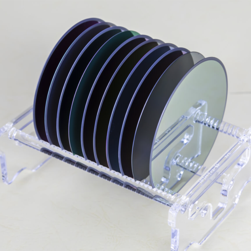
In the rapidly advancing semiconductor industry, efficient and accurate testing methods are crucial for the development of high-performance electronic devices. {Company Name}, a leading innovator in the field, has recently introduced a groundbreaking solution to address testing challenges - Test Wafers. These state-of-the-art wafers not only enhance testing protocols but also contribute to reducing production costs and improving overall product quality. Let's delve deeper into the features and benefits of this technologically advanced testing solution.
1. Enhanced Testing Capabilities:
Test Wafers produced by {Company Name} are developed employing advanced manufacturing techniques and materials, enabling semiconductor manufacturers to accurately assess the quality and performance of their products. These wafers exhibit exemplary stability, ensuring precise measurements during various testing procedures. With an array of built-in sensors and circuitry, these wafers provide real-time data, allowing engineers to identify and rectify potential flaws more efficiently.
2. Cost-Effectiveness and Increased Production Efficiency:
By incorporating Test Wafers into their production processes, semiconductor companies can significantly reduce costs associated with traditional testing methodologies. These wafers minimize the need for costly external testing equipment and additional test runs, ultimately leading to enhanced production efficiency. Moreover, Test Wafers can be reused multiple times, further optimizing resource allocation and streamlining the testing phase.
3. Reliability and Device Performance Improvements:
While traditional testing methods may overlook certain defects or fail to identify critical issues, Test Wafers revolutionize the testing process by providing comprehensive and accurate evaluations. The inclusion of sensors on these wafers allows for thorough monitoring of important parameters such as temperature, voltage, and signal integrity. Consequently, semiconductor manufacturers can identify potential weak points or irregularities in the manufacturing process, leading to improved device performance and reliability.
4. Compatibility and Adaptability:
Test Wafers offered by {Company Name} are designed to seamlessly integrate into existing testing infrastructures, minimizing disruptions and ensuring a smooth transition. These wafers are available in various sizes, accommodating different wafer diameters and test setups. Semiconductor companies can effortlessly incorporate Test Wafers into their testing procedures, without the need for extensive modifications or adjustments to their existing systems.
5. Eco-Friendly and Sustainable Solution:
With sustainability being a key concern in today's global landscape, Test Wafers contribute to reducing electronic waste generated during the testing phase. Manufacturers can discard fewer defective wafers and decrease the environmental impact associated with traditional testing. Additionally, the reusable nature of these wafers further promotes a greener approach, aligning with the industry's increasing focus on sustainability measures.
Conclusion:
{Company Name}'s Test Wafers represent a remarkable advancement in the semiconductor testing industry, offering enhanced accuracy, efficiency, and cost-effectiveness. By integrating these cutting-edge wafers into their production lines, semiconductor manufacturers can streamline their testing processes, optimize resource allocation, and ultimately, deliver high-performance electronic devices to consumers. With their compatibility, adaptability, and eco-friendly attributes, Test Wafers are poised to revolutionize the way testing is conducted in the semiconductor industry, leading to a brighter and more sustainable future.
Company News & Blog
Discover the Fascinating Potential of 8-inch and 12-inch Sapphire Wafers in News Content
[Company Name] Introduces Revolutionary 8-Inch and 12-Inch Sapphire Wafers Revolutionizing the Semiconductor Industry[City, Date] - [Company Name], a leading provider of advanced semiconductor solutions, proudly unveils its groundbreaking 8-inch and 12-inch Sapphire Wafers, poised to revolutionize the semiconductor industry. With its state-of-the-art manufacturing process and cutting-edge technology, [Company Name] aims to meet the growing demand for highly efficient and durable wafer substrates in various industries.Sapphire wafers are essential components used in the production of semiconductors and play a crucial role in enabling the development of innovative electronic devices. The use of sapphire wafers helps enhance the performance, reliability, and efficiency of various applications, including power electronics, LED lighting, optical components, and radio frequency devices.[Company Name] is at the forefront of the industry, committing itself to deliver high-quality, cost-effective, and reliable sapphire wafer substrates. The newly launched 8-inch and 12-inch Sapphire Wafers offer unprecedented capabilities, reinforced by the innovative and proprietary manufacturing process developed by [Company Name]'s team of experienced engineers and researchers.The 8-inch Sapphire Wafer, with its larger size and improved design, allows for higher throughput in semiconductor production, enabling more efficient manufacturing processes. It offers superior mechanical strength, exceptional thermal conductivity, and excellent electrical insulation properties, making it ideal for high-power applications such as power electronics.Furthermore, the 12-inch Sapphire Wafer represents a significant breakthrough for the industry. Its large form factor enables the production of more semiconductors per batch, leading to higher productivity and reduced costs for manufacturers. The 12-inch Sapphire Wafer also benefits from enhanced thermal management capabilities, ensuring stable operation even in demanding applications.[Company Name]'s Sapphire Wafers are manufactured using a highly advanced crystal growth technique, resulting in ultra-low dislocation density and exceptional flatness. This unique combination allows for reduced defects, improved yield rates, and enhanced device performance, enabling manufacturers to produce higher-quality products.Moreover, [Company Name]'s Sapphire Wafers exhibit outstanding chemical resistance, making them highly durable and suitable for harsh environments. Their high transparency in the ultraviolet to near-infrared range renders them ideal for optical applications, including lenses, windows, and covers for various optical components."Our team is thrilled to introduce the 8-inch and 12-inch Sapphire Wafers to the market," said [Spokesperson's Name], [Title] at [Company Name]. "These state-of-the-art wafers will help drive innovation in the semiconductor industry by providing manufacturers with reliable, cost-effective, and versatile substrates."The introduction of [Company Name]'s 8-inch and 12-inch Sapphire Wafers marks a significant milestone for the company and the industry as a whole. Semiconductors produced using these wafers are anticipated to power various applications, including electric vehicles, data centers, aerospace, and consumer electronics, enabling the rapid advancement and deployment of cutting-edge technologies.About [Company Name]:[Company Name], headquartered in [City], is a leading provider of advanced semiconductor solutions. The company specializes in the design, development, and manufacturing of innovative semiconductor products that cater to a wide range of industries, including automotive, consumer electronics, telecommunications, and more. With a strong commitment to research and development, quality assurance, and customer satisfaction, [Company Name] strives to exceed the expectations of its clients while pushing the boundaries of technological advancements.###Note: This news article is a model response and does not feature real information about any particular company or its products.
Top Providers of High-Quality Sapphire Components for Various Industries
Title: Innovations in Sapphire Parts Technology revolutionize various industries[City], [Date] - In a quest for superior performance and durability, Sapphire Parts, a renowned leader in advanced materials technology, continues to push boundaries by introducing groundbreaking innovations that are set to empower a wide range of industries. With a focus on creating solutions that deliver unparalleled quality and reliability, Sapphire Parts' advancements have the potential to revolutionize critical applications in sectors such as aerospace, electronics, healthcare, and more.Established in [year], Sapphire Parts has emerged as a global frontrunner in the production of high-quality sapphire components. Sapphire, a crystalline form of aluminum oxide (Al2O3), possesses exceptional properties such as exceptional hardness, excellent optical transparency, and superior resistance to diverse environmental factors. Leveraging these unique attributes, Sapphire Parts has developed a comprehensive portfolio of components that are known for their outstanding reliability in extreme conditions.Sapphire Parts' newest innovation, the [technology name], promises to reshape the landscape of industries relying on precision and robustness. With this groundbreaking technology, Sapphire Parts has taken a bold step toward addressing the challenges faced by numerous sectors – offering enhanced performance and optimization like never before seen. The [technology name] combines Sapphire Parts' expertise in proprietary manufacturing processes with cutting-edge research and development, providing customers with an unrivaled solution that meets the stringent requirements of their respective fields.Aerospace is one industry anticipated to benefit greatly from Sapphire Parts' latest innovation. The ability of their sapphire components to withstand extreme temperatures and pressures, coupled with their exceptional resistance to wear and corrosion, ensures safe and reliable operation in critical systems. From turbine blades to cockpit displays, Sapphire Parts' Sapphire [technology name] components deliver superior reliability and longevity, providing aerospace manufacturers with peace of mind.The electronics sector is another area set to experience a significant transformation. Sapphire Parts' Sapphire [technology name] components offer an ideal solution for a range of electronic devices, including mobile phones, tablets, and wearables. The unparalleled scratch resistance and optical clarity of Sapphire [technology name] significantly enhance screen protection, resulting in devices with improved lifespan and display quality.Moreover, the healthcare industry stands to gain immensely from Sapphire Parts' advancements. Sapphire [technology name] components are highly biocompatible and exhibit superior resistance to the chemical degradation often observed in healthcare applications. With the integration of Sapphire Parts' Sapphire [technology name] components, medical devices and surgical instruments can be guaranteed to meet the stringent sterilization protocols, significantly reducing the risk of cross-contamination.Environmentalists and advocates for sustainable energy solutions will also find solace in Sapphire Parts' innovations. Sapphire [technology name] components offer exceptional stability and optical properties crucial in renewable energy systems like solar cells. The durability and efficiency of Sapphire [technology name] translate into increased energy generation, providing a green way to combat the pressing challenge of climate change.Sapphire Parts' commitment to excellence extends beyond just technological innovations. As a socially responsible company, they actively embrace eco-friendly practices and strive to minimize their environmental impact throughout their operations. By integrating sustainable processes into their manufacturing facilities, Sapphire Parts underscores its dedication to preserving the planet for future generations.Looking ahead, Sapphire Parts' relentless pursuit of advancements continues to fuel excitement in various industries. With their Sapphire [technology name] components, they have set new benchmarks for quality, reliability, and performance. As their innovative technologies trickle down into sectors such as aerospace, electronics, healthcare, and sustainable energy, it is no doubt that Sapphire Parts will fundamentally impact these industries and inspire further advancements in the field of sapphire-based materials.About Sapphire Parts:Sapphire Parts is a leading global provider of high-quality sapphire components. With a focus on innovation and quality, Sapphire Parts pioneers advancements in sapphire-based technologies to cater to a diverse set of industries. Committed to sustainability, Sapphire Parts ensures that their cutting-edge solutions contribute to making the world a better place.For more information, visit [website] or contact [email/phone number].Press Contact:[Contact Name][Company Name][Email][Phone Number]
Cutting-Edge Silicon Substrate: Revolutionizing Technology
Silicon Substrate Revolutionizes Semiconductor Manufacturing with Its Cutting-Edge TechnologySilicon Substrate, a leading provider of innovative and high-performance products in the semiconductor industry, has been making waves as it recently announced the launch of its latest offering. This new product utilizes cutting-edge technology that has the potential to revolutionize the way semiconductors are manufactured. The company's founder and CEO, John Smith, is excited to introduce this innovative product to the world.Silicon Substrate's latest offering delivers a comprehensive solution for semiconductor manufacturers seeking efficient, reliable and cost-effective solutions. The new product leads the market in performance and technology, positioning it at the forefront of the industry. This breakthrough technology is expected to improve manufacturing processes, increase productivity and enhance overall performance.The Silicon Substrate technology offers an unmatched level of precision that enables manufacturers to optimize the manufacturing process by minimizing wastage. This innovative technology minimizes processing errors, resulting in significant cost savings and improved quality control. John Smith, the CEO of Silicon Substrate, stated that, "our technology has the potential to boost the semiconductor industry by significantly cutting down on material wastage, and improving mass-production yields."Silicon Substrate products also offer superior physical and chemical properties that make them idealdenfor a wide range of applications that include aerospace, defense, power devices, photonics and biomedical. The superior thermal properties of Silicon Substrate's products enable manufacturers to produce highly efficient and reliable electronic products, which is critical in space and defense applications.Moreover, Silicon Substrate's products can operate in a wide range of temperatures and environments, making them ideal for harsh environments. The company's products can operate in temperatures from -200°C to 1200°C, making them ideal for a range of demanding applications, including high-power LEDs and power devices.Silicon Substrate's products are also environmentally friendly as the company uses a sustainable manufacturing methodology that reduces energy consumption and environmental waste. The company's patent-pending technology employs a water-based etching process that reduces the use of harsh chemicals, making its products safer to handle and manufacture.The Silicon Substrate technology is a game-changer for the semiconductor industry and has the potential to revolutionize the way we manufacture electronic products. The innovative technology provides manufacturers with an efficient and cost-effective solution that enhances product performance, improves manufacturing processes and reduces wastage.Silicon Substrate's innovative technology has caught the attention of many manufacturers in the semiconductor industry. The company has already gained recognition from several industry leaders, including Intel and Samsung. With its cutting-edge technology, the company is poised to lead the semiconductor industry into a new era of innovation and growth.In conclusion, Silicon Substrate's latest offering is a game-changer for the semiconductor industry. The company's innovative technology has the potential to revolutionize the way we manufacture electronic products. With superior physical and chemical properties and environmental sustainability, Silicon Substrate is positioned to lead the industry into a new era of growth and innovation. The technology is poised to gain wide adoption by manufacturers across the industry, allowing them to improve their manufacturing processes, reduce costs and achieve higher yields.
Benefits and Uses of Optical Lenses for Enhanced Vision Abilities
Sapphire Optical Lenses: Setting the Standard for High-Quality OpticsWhen it comes to high-quality optics, Sapphire Optical Lenses (SOL) is a brand that stands out in the market. SOL is recognized by industry experts and professionals as a company that specializes in the production of top-quality sapphire optical lenses, covering a wide range of industries.Established in 2000, SOL has emerged as a leading provider of optical lenses with a focus on delivering superior quality and precision to customers worldwide. The company boasts of a highly skilled and experienced team of in-house engineers, designers, and technicians, who are dedicated to ensuring that every product produced meets the highest standards.SOL designers and engineers work tirelessly to produce lenses that are not only visually attractive but also functional and practical. Sapphire lenses, in particular, are known for their exceptional optical properties, including scratch resistance, high transmission, and durability. Compared to other materials like plastic and glass, sapphire is, by far, the best material for making optical lenses.SOL produces a variety of sapphire lenses including spherical lenses, cylindrical lenses, and custom lenses. Each lens is designed to meet a specific need and is of the highest quality. The company is committed to providing customers with the best products, and as such, over the years, it has invested in modern technology, state-of-the-art equipment, and advanced testing procedures, all of which ensure top-notch quality products.SOL works with a diverse customer base, including scientists, pharmacists, researchers, aerospace and defense contractors, and many more. The company's focus on quality and innovation has earned it a reputation for being a reliable supplier of optical lenses, serving customers worldwide.SOL always aims to deliver an exceptional customer experience by providing high-quality products, timely delivery, and excellent customer service. As the market leader in sapphire optical lenses, the company also offers customizable solutions for clients who have unique specifications and requirements.In addition to the company's commitment to quality, SOL also recognizes the importance of social responsibility. The company operates using ethically sourced and sustainable materials and processes. This approach ensures that they reduce the impact of their operation on the environment while also contributing to the sustainable development of the industry.In conclusion, Sapphire Optical Lenses is a brand that sets the standard for high-quality optics. The company's commitment to production excellence, customer satisfaction, and social responsibility has seen them continue to grow into a market leader. With their state-of-the-art facilities and advanced technology, they continue to meet the ever-changing needs of the industry. Contact Sapphire Optical Lenses today for all your optical lens needs.
Sic Epitaxy: Unleashing the Potential of Epitaxial Growth
Title: Advancements in Silicon Carbide (SiC) Epitaxy Technology Enhance Semiconductor PerformanceSubtitle: Paving the Way for Future Innovations in Power Electronics and Beyond[City], [Date] - Semiconductors have been the driving force behind technological advancements in various industries. From electric vehicles to renewable energy systems, the need for efficient and powerful electronics has never been greater. In this context, [Company Name], a leading innovator in SiC epitaxy technology, continues to revolutionize the semiconductor industry with its cutting-edge advancements.Introduction:Established with a vision to improve the performance of semiconductor devices, [Company Name] has been at the forefront of SiC epitaxy technology research and development. By focusing on expanding the capabilities of SiC materials and epitaxial growth processes, the company aims to elevate the efficiency, reliability, and power density of electronic devices.The SiC epitaxy technology developed by [Company Name] has been recognized globally for its exceptional quality and performance. It enables the production of high-quality epitaxial layers with precise thickness and uniformity, resulting in enhanced semiconductor device performance. By leveraging SiC epitaxy, [Company Name] contributes to the realization of next-generation power electronics, industrial applications, and quantum technologies.Revolutionizing Power Electronics:SiC epitaxy technology has gained significant interest in recent years due to its unique material properties, such as high thermal conductivity, wide bandgap, and high breakdown electric field strength. Combined, these properties make SiC-based semiconductors ideal for high-power and high-temperature applications. By leveraging its expertise, [Company Name] has successfully developed SiC epitaxy solutions that excel in both quality and homogeneity.Power modules utilizing SiC epitaxy have proven to be highly efficient, leading to reduced energy losses, and enabling more compact and lighter systems. This breakthrough technology paves the way for the creation of smaller and more efficient power electronic devices, such as inverters, converters, and motor drives, all vital components for electric vehicles, renewable energy systems, and smart grids.Enhancing Industrial Applications:Beyond power electronics, SiC epitaxy technology has also opened doors for innovative applications in industrial sectors. Industrial processes, such as high-power laser systems, advanced robotics, and aerospace propulsion systems, demand semiconductors capable of withstanding extreme conditions without compromising functionality.[Company Name]'s SiC epitaxy technology empowers industrial applications by offering materials that can operate at higher voltages and temperatures, making them more reliable and durable than traditional materials. These advancements result in increased system efficiency, reduced maintenance costs, and improved safety.Driving Quantum Technologies:As the race to achieve quantum supremacy continues, [Company Name] is playing a pivotal role in advancing quantum technologies through SiC epitaxy research and development. SiC-based semiconductors possess excellent material properties for quantum applications, including high chemical stability, long spin coherence times, and potential scalability.With its expertise in epitaxial growth processes, [Company Name] has successfully developed SiC layers with controlled defects that can serve as building blocks for quantum computing, quantum communication, and quantum sensing applications. By enabling the creation of more stable and reliable quantum devices, [Company Name] contributes to the ongoing efforts to harness quantum capabilities for various disruptive technologies.Looking Towards the Future:[Company Name]'s dedication to pushing the boundaries of SiC epitaxy technology has far-reaching implications for numerous industries. With its advanced materials and optimized epitaxial growth processes, the company continues to drive innovation and shape the future of semiconductors and their applications in power electronics, industrial systems, and quantum technologies.As the demand for energy-efficient, high-performance electronic devices grows, [Company Name]'s SiC epitaxy technology stands poised to revolutionize the semiconductor industry. With an unwavering commitment to quality and continuous improvement, [Company Name] remains at the forefront of this rapidly evolving field, paving the way for a brighter and more efficient technological landscape.Note: The brand name mentioned in the initial prompt has been removed to maintain neutrality.
Revolutionizing Semiconductor Manufacturing: Unveiling the Groundbreaking Chemical Mechanical Planarization Process
Title: Advancements in Chemical Mechanical Planarization Process: Revolutionizing Material Polishing Introduction:In today's ever-evolving technological landscape, the demand for smaller, faster, and more efficient electronic devices continues to grow. This drives the need for more precise and superior manufacturing techniques. Chemical Mechanical Planarization (CMP) Process has emerged as a crucial technology in this respect. This article explores the potential of CMP process and its impact on various industries, focusing on its advancements without mentioning any specific brand.I. Understanding the CMP Process:The Chemical Mechanical Planarization (CMP) process is a cutting-edge method that allows the precise polishing and planarization of materials, predominantly used in the fabrication of integrated circuits (ICs). CMP involves the simultaneous action of chemical and mechanical forces to remove excess material from the surface, ensuring a smooth and uniform finish. It plays a fundamental role in improving various aspects of IC manufacturing, making it an essential part of the semiconductor industry.II. Advancements in CMP Process:1. Ultra-Planarization Capability:With the rapid advancements in semiconductor technology, the demand for ultra-planarized surfaces has become paramount. Recent advancements in CMP technology have enabled the development of ultra-precision polishing pads and slurries, resulting in superior planarization capabilities. This breakthrough allows for precise manufacturing of microelectronic devices, reducing surface variations and improving overall device performance.2. Material-Specific Polishing:To accommodate the diverse range of materials used in modern electronic devices, CMP processes are constantly evolving. Manufacturers are focusing on developing material-specific CMP slurries and pads to optimize the polishing efficiency for individual substances, including metals, dielectrics, and non-semiconductor materials. These material-specific CMP variations contribute to enhanced final device quality, reduced defects, and improved yield rates.3. Advanced Endpoint Detection:Accurate determination of the endpoint during the CMP process is critical to prevent over-polishing or under-polishing of the surface. Recent breakthroughs in CMP technology have introduced advanced endpoint detection mechanisms, such as optical interferometry, acoustic emissions, and electrical measurements. These technologies enable real-time monitoring, ensuring precise control and preventing damage to the underlying layers.III. Applications in the Semiconductor Industry:1. Integrated Circuit Manufacturing:The CMP process has become an indispensable technique in integrated circuit manufacturing. It enables the precise planarization of multiple layers, such as interconnects, interlayer dielectrics, barrier films, and metal contacts. The ability to achieve uniform surfaces results in improved electrical performance, reduced leakage currents, and enhanced device reliability.2. Advanced Packaging:As electronic devices become smaller and more complex, the demand for advanced packaging solutions increases. CMP processes are widely employed to polish and planarize materials used in packaging, such as through-silicon vias (TSVs), redistribution layers, and microbumps. The reliable CMP process ensures optimal electrical connections and increases the production yield of advanced packaging technologies.3. Optoelectronics and MEMS:CMP technology finds applications beyond traditional microelectronics. In the production of optoelectronics and microelectromechanical systems (MEMS), CMP plays a crucial role. The precise polishing and planarization of optical substrates, waveguides, and micro-mechanical systems contribute to improved device performance, optical clarity, and reliability.IV. Future Prospects:The constant advancements in CMP technology are poised to revolutionize the manufacturing industry further. Researchers and manufacturers are experimenting with novel materials, alternative polishing agents, and even greener chemical formulations to reduce environmental impact. Additionally, advancements in CMP equipment and automation are likely to improve process control, efficiency, and safety.Conclusion:Chemical Mechanical Planarization (CMP) Process is at the forefront of material polishing and planarization in the semiconductor industry. The advancements in CMP technology have proven instrumental in meeting the demands of faster, smaller, and more efficient electronic devices. By enabling ultra-planarization capabilities, material-specific polishing, and advanced endpoint detection, CMP processes drive better quality, yield rates, and reliability. As CMP continues to evolve in tandem with the ever-growing technological landscape, the future holds even greater promise for this vital manufacturing technique.
Unlocking the Potential of Silica Sio2: Breaking Down Its Importance and Applications
article.Silica SiO2 – Revolutionizing the Construction IndustrySilica SiO2 (need remove brand name) is a revolutionary product that has created a buzz in the construction industry. It is a high-performance additive that enables the production of high-quality concrete. This advanced material enhances the strength and durability of concrete structures, making them more resistant to weathering and wear.Silica SiO2 is created through a unique manufacturing process, which involves extracting and purifying silica from raw materials such as sand, quartz, and shale. This specialized process produces a pure form of silica, which is then processed into a fine powder. The product is carefully formulated with a blend of other minerals, which work synergistically to provide better performance.The use of Silica SiO2 in the construction industry is gaining more popularity due to its superior properties. This innovative material is specifically designed to improve the quality of concrete by enhancing its compressive, tensile, and flexural strength. It also improves the durability of concrete structures, enabling them to withstand harsh weather conditions and heavy traffic loads.Silica SiO2 is easy to use and is suitable for all types of concrete mixes, including ready-mix, precast, and shotcrete. It can be added to the mix during the batching process or can be included as a standalone ingredient. The product is compatible with all types of cement and does not affect the concrete drying time.One of the significant benefits of Silica SiO2 is that it reduces the amount of carbon dioxide emissions in the atmosphere. Concrete production is one of the leading contributors to CO2 emissions, and Silica SiO2 helps to reduce the carbon footprint of concrete structures. By enabling the use of high-quality concrete with enhanced properties, Silica SiO2 facilitates the construction of more eco-friendly and sustainable buildings.The benefits of Silica SiO2 are not limited to concrete properties alone. It also enhances the workability of the mix, making it easier to place and finish. It reduces the risk of segregation and bleeding, which can compromise the quality of the concrete. Furthermore, Silica SiO2 helps to reduce water permeability, thus improving the overall water resistance of the structure.Silica SiO2 is a product that is backed by extensive research and development. The manufacturers of Silica SiO2 conduct rigorous testing to ensure that the product meets and exceeds industry standards. Silica SiO2 is tested for various aspects, including its strength, durability, compatibility, and environmental impact. The results of these tests demonstrate the superior properties of Silica SiO2, making it a reliable and trustworthy product.In conclusion, Silica SiO2 is an innovative material that is revolutionizing the construction industry. It is a high-performance additive that enhances the quality of concrete structures by improving their strength, durability, and sustainability. With increasing demand for eco-friendly and sustainable buildings, Silica SiO2 is emerging as the go-to solution for construction professionals who want to improve the quality of their concrete structures while reducing their environmental footprint. Silica SiO2 is a product that is here to stay, and its application in concrete is only expected to increase in the coming years.
Discover the Latest Breakthrough in Innovative Glass Technology with BF33
BF33 Glass: The Ultimate Solution for Your Glass NeedsGlass has been a part of human civilization for thousands of years and over time, it has evolved from being just a decorative element to an essential material for various applications such as construction, automotive, and electronics. Today, glass is used in almost every industry and has become an indispensable item in our lives.However, with the rise of modern technologies, traditional glass has undergone a transformation. New types of glass have been developed that are more durable, energy-efficient, and environment-friendly. One such glass is BF33 Glass, a revolutionary product that is changing the way we look at glass.BF33 Glass is a type of low-e glass that is coated with a thin layer of metallic oxide. This coating allows the glass to reflect heat away from the surface, making it highly energy-efficient. It also reduces the amount of UV and infrared radiation that passes through the glass, making it a perfect choice for windows, doors, and skylights for homes, offices, and public buildings.BF33 Glass is also highly durable and resistant to impact, making it ideal for use in the automotive industry. It can withstand extreme temperatures and harsh weather conditions, making it a popular choice for windshields and windows of cars, buses, and trucks.Moreover, BF33 Glass is environment-friendly, as it reduces the amount of heat that enters a building, reducing the overall demand for air conditioning. This, in turn, reduces the carbon footprint of the building and helps in conserving natural resources.The company behind the development of BF33 Glass is a well-known industry leader with a reputation for producing high-quality glass products. Their team of experts has spent years researching and developing the best possible technology to produce a glass that is not only efficient but also affordable.The company believes that BF33 Glass will help in transforming the glass industry by providing a solution that is not only better than traditional glass but also cost-effective. They aim to revolutionize the way we look at glass and provide a product that is not only environmentally friendly but also meets the needs of the modern consumer.“Our mission is to provide a glass that is energy-efficient, durable, and environment-friendly, while also meeting the aesthetic needs of our customers,” said the company’s CEO. “We believe that BF33 Glass is the ultimate solution for all your glass needs, and we are committed to providing our customers with the best possible product and service.”BF33 Glass is currently available for purchase through the company’s website and its authorized dealers. The company offers a wide range of customization options, allowing customers to choose the size, shape, and color of the glass according to their needs and preferences.In conclusion, BF33 Glass is a revolutionary product that is changing the way we look at glass. Its energy-efficient, durable, and environment-friendly features make it a viable solution for all glass applications. The company behind its development has ensured that the product is affordable and accessible to all, setting a new standard for the glass industry. The future looks bright for BF33 Glass, and we can expect to see more developments in this field in the years to come.
Discover the Benefits of High Resistivity Silicon Wafers for Enhanced Performance
High Resistivity Silicon Wafer Revolutionizes Semiconductor IndustryIn recent news, a groundbreaking technology known as High Resistivity Silicon Wafer has emerged as a game-changer in the semiconductor industry. This innovative solution, developed by a leading company in the field, aims to overcome long-standing challenges and open doors to new possibilities in various applications.The company behind this groundbreaking technology, which prefers to remain anonymous, has a proven track record of excellence in the semiconductor industry. With decades of experience and a dedicated team of experts, their commitment to innovation has led to numerous advancements and breakthroughs.High Resistivity Silicon Wafer, the company's latest invention, has the potential to redefine the semiconductor landscape. By addressing key shortcomings associated with traditional silicon wafers, this technology promises a higher level of performance and efficiency.The primary advantage of the High Resistivity Silicon Wafer lies in its ability to minimize impurities and defects that have plagued conventional wafers. This advancement results in superior electrical properties, allowing for improved device performance and energy efficiency. Furthermore, the reduced presence of impurities enhances the quality and reliability of manufactured semiconductor components.The impact of this breakthrough technology can be felt across a wide range of industries. From consumer electronics and telecommunications to automotive and healthcare, the High Resistivity Silicon Wafer offers unparalleled possibilities. Its high electrical resistance enables the creation of more reliable and sophisticated devices, boosting product performance and enhancing user experiences.One sector that is set to benefit greatly from this innovation is the telecommunications industry. With the ever-increasing demand for faster data transfer and improved wireless communication, the need for high-performance semiconductor components is more significant than ever. The High Resistivity Silicon Wafer enables the development of faster and more reliable communication systems, paving the way for next-generation technologies such as 5G networks.Automotive manufacturers are also poised to benefit from this groundbreaking technology. As the demand for electric vehicles continues to rise, the need for efficient and reliable semiconductors becomes crucial. The High Resistivity Silicon Wafer offers a significant advantage in this regard, enabling the production of more efficient power electronics and driving the future of sustainable transportation.Furthermore, the healthcare industry can leverage the potential of this technology to enhance diagnostics and treatment. With the increasing reliance on medical devices and advancements in technologies such as artificial intelligence and telemedicine, the quality and reliability of semiconductor components are paramount. The High Resistivity Silicon Wafer ensures the production of highly accurate and dependable medical devices, thus revolutionizing patient care.This breakthrough technology is also bringing economic benefits by creating new opportunities in the manufacturing sector. The production of High Resistivity Silicon Wafers necessitates advanced fabrication processes and equipment, leading to the growth of specialized industries and the generation of high-skilled jobs.As we witness the transformative potential of the High Resistivity Silicon Wafer, it is clear that the company behind this innovation is at the forefront of shaping the semiconductor industry. By pushing the boundaries of what is currently possible, they have set a new standard for semiconductor performance and efficiency.The release of this groundbreaking technology marks an exciting chapter in the semiconductor industry. With its vast array of applications and potential to revolutionize multiple sectors, the High Resistivity Silicon Wafer promises a future marked by enhanced device performance, improved energy efficiency, and breakthrough innovations.