
New Glass Material BF33 Offers Enhanced Durability and Clarity
By:Admin
The BF33 Glass is a result of years of research and development, as the company continuously strives to push the boundaries of what is possible in glass manufacturing. The product’s composition and design have been carefully engineered to provide superior strength and resistance to impact, making it suitable for a wide range of applications.
One of the key features of BF33 Glass is its exceptional transparency, which allows for maximum light transmission. This makes it an ideal choice for architectural and building applications, where natural light is a significant factor in design. Additionally, its high clarity and low distortion properties make it an excellent choice for display screens and digital signage.
Moreover, BF33 Glass offers outstanding resistance to scratches, abrasion, and chemical damage, making it a highly durable and long-lasting material. This makes it an excellent choice for use in high-traffic areas, such as retail stores, museums, and public facilities, where maintaining a pristine appearance is crucial.
Furthermore, BF33 Glass has been designed to meet stringent safety standards, making it an ideal choice for use in automotive and aerospace applications. Its exceptional impact resistance and shatterproof properties make it a reliable choice for use in vehicle windshields, windows, and other structural components.
The company has also emphasized the environmental benefits of BF33 Glass, as it is fully recyclable and manufactured using sustainable practices. This commitment to sustainability aligns with the company's dedication to reducing its environmental impact and promoting eco-friendly products.
In addition to its practical applications, BF33 Glass also offers a range of design possibilities due to its versatility. Its ability to be molded and shaped into various forms opens up opportunities for creative and innovative uses in architecture, interior design, and product development.
The introduction of BF33 Glass has already garnered attention from various industries, with early adopters expressing great enthusiasm for its potential. Architects, engineers, designers, and manufacturers are eager to incorporate this cutting-edge material into their projects, seeing it as a way to enhance both the aesthetic and functional aspects of their creations.
The company is currently working with strategic partners to bring BF33 Glass to market, and is actively engaging with potential customers to demonstrate the numerous advantages of this groundbreaking material. The company's commitment to providing exceptional customer service and support ensures that clients will have access to the necessary resources and expertise to implement BF33 Glass in their projects successfully.
Overall, the introduction of BF33 Glass represents a significant advancement in the field of glass technology, offering unmatched performance and versatility. With the potential to revolutionize industries ranging from construction and automotive to electronics and design, BF33 Glass is poised to make a lasting impact and set a new standard for high-performance glass products.
Company News & Blog
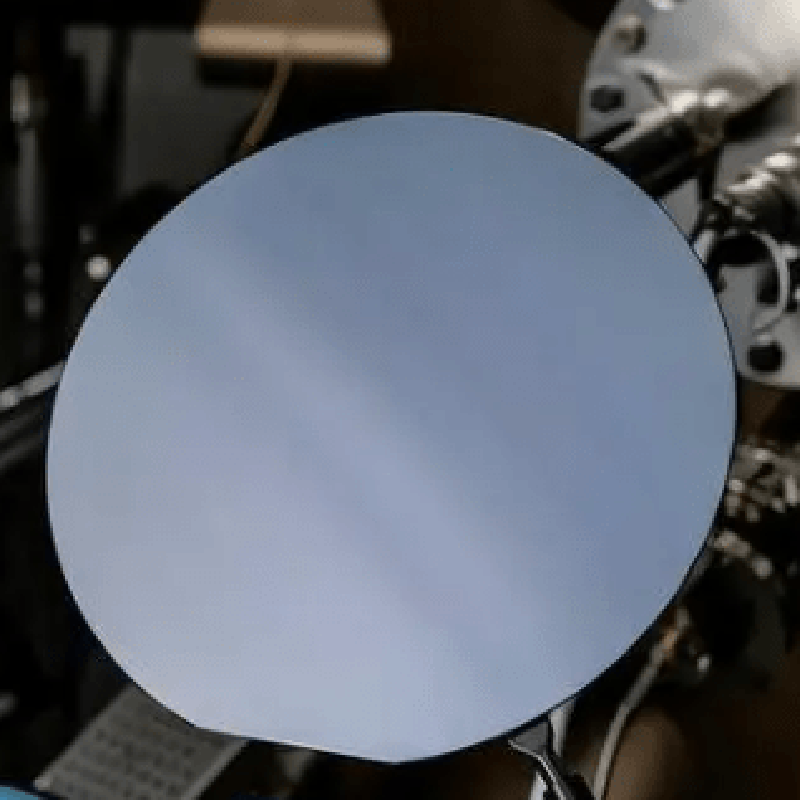
Breakthrough in Crystalline Material: SrTiO3 Wafer Holds Potential for Revolutionary Applications
A new technology using SrTiO3 wafers promises to revolutionize the semiconductor industry by improving the efficiency and performance of electronic devices. SrTiO3 is a unique material with exceptional electrical and optical properties that make it ideal for use in electronic devices such as computers, smartphones, and other digital devices.SrTiO3 is a complex oxide compound made up of Strontium, Titanium, and Oxygen. It exhibits semiconducting properties, which is why it’s relevant to the electronics industry. The technology is particularly useful in the development of advanced semiconductor devices such as MOSFETs, solar cells, and transistors, among others.SrTiO3 wafers have been in use in the semiconductor industry for years, but scientists have been exploring ways to make the compound material more efficient and precise. New research shows that combining SrTiO3 with other materials, such as hafnium oxide, can produce even more remarkable results.The company behind this breakthrough development is a leading producer of high-quality wafers for the electronics industry. The company has been a pioneer in the development of semiconductor-grade crystals, and its technological advancements continue to push the boundaries of what is possible within the industry.The SrTiO3 wafer technology has significant implications for the future of the electronics industry. Manufacturers can use the technology to develop devices that are more powerful, efficient, and affordable. The use of SrTiO3 wafers in the manufacturing process ensures that electronic components are more reliable and can operate at higher temperatures.The technology also has significant benefits for solar cell technology. SrTiO3-based solar cells have higher conversion efficiencies than conventional cells, making them more desirable for use in photovoltaic systems. The use of this technology in solar panels could lead to the development of more efficient and cost-effective solar panels, helping bring clean energy to millions of people worldwide.The innovative SrTiO3 wafer technology has many applications, including in the automotive, healthcare, and aerospace industries. Researchers are exploring new uses for the technology and hope to discover new applications that will further revolutionize the electronics industry in the coming years.The company's patented manufacturing process for SrTiO3 wafers ensures the production of high-quality materials that meet strict industry standards. The company's wafers are currently being used in research and development laboratories around the world, and several companies have already adopted the technology in their manufacturing processes.The use of SrTiO3 wafers in electronic devices is set to increase in the coming years as the technology becomes more widespread and affordable. The introduction of this technology has significant implications for the electronics industry, and researchers are excited by its potential to transform the industry's future.In conclusion, the emergence of SrTiO3 wafers has set the semiconductor industry on a path towards a new generation of electronic devices. The technology has significant implications for the development of powerful, efficient, and affordable electronic devices, solar cell technology, and many other applications. With continued research and development, the technology has the potential to revolutionize the electronics industry for years to come.
Discover the Latest Advances in Insulator and Semiconductor Technologies
Insulator and Semiconductor Combine Strengths to Enhance Technology InnovationInsulator and Semiconductor, two high-tech companies, announced that they have combined their strengths to deliver more comprehensive technology solutions to the market. With a shared passion for innovation and a commitment to excellence, the partnership enables these companies to increase their collective capabilities and bolster their competitive edge.Insulator and Semiconductor share a focus on developing cutting-edge technologies that drive progress in diverse industries. Both companies excel in developing application-specific integrated circuits (ASICs) that are tailored to meet specific customer requirements. Insulator is known for its expertise in high-precision analog and mixed-signal IC design, as well as its high-reliability product manufacture. On the other hand, Semiconductor contributes to the partnership with its specialization in power electronics and embedded computing systems.The combination of Insulator and Semiconductor provides customers with an unparalleled set of technology offerings, spanning the entire spectrum of digital and analog design and manufacturing. Their collaboration benefits not only the product end-users but also OEMs, who can leverage the technology know-how of the two companies to develop customized ASICs that better meet their needs.The partnership between Insulator and Semiconductor brings together advantages of both individual companies in the realm of innovation, speed to market, and flexibility. The complementary nature of their expertise also helps them to tackle emerging challenges in the field of ASIC design, such as cost optimization and eco-friendliness. By joining forces, the companies can enhance their technological know-how and R&D infrastructure to stay at the forefront of the industry.“Insulator and Semiconductor have long shared similar philosophies and values when it comes to innovation and business excellence,” says Alex Chen, CEO of Insulator. “This partnership enables us to combine our strengths and be better positioned to offer our customers comprehensive, high-quality solutions that they can rely on.”When combined, the expertise of the two companies enhances not only ASIC design but also product lifecycles, from conceptualization to deployment, support and upgrading. The partnership has a shared objective of creating more efficient, reliable, and eco-friendly technology solutions for the global market.“By bringing together the strengths of two innovative companies, we will be able to provide our clients with deeper, more nuanced knowledge and skills to drive efficiency and productivity gains,” adds Frank Wu, CEO of Semiconductor. “The complementary nature of our expertise will readily translate to market-leading products and services that will shape the industry and benefit our clients in the years to come.”Insulator and Semiconductor are dedicated to keeping their customers up to date with the latest technology advances for their products, and the partnership will encourage continued progress in these respects. With greater shared expertise and commitment to innovation, Insulator and Semiconductor will delight customers with superior products and services, driving progress throughout the industry.
Exploring the Latest Developments in Semiconductor Materials
Semiconductor Manufacturers, a leading global manufacturer of semiconductor materials, has recently announced the launch of its latest product line aimed at revolutionizing the field of semiconductor technology. The company's innovative materials are poised to enhance the performance and efficiency of electronic devices, from consumer electronics to industrial applications.With a history of over 30 years in the semiconductor industry, Semiconductor Manufacturers has established a reputation for delivering high-quality materials that meet the stringent requirements of semiconductor manufacturers. The company's extensive portfolio of materials includes silicon wafers, epitaxial wafers, and advanced packaging materials, all of which play a critical role in the production of cutting-edge electronic devices.Semiconductor Manufacturers has a strong commitment to research and development, investing heavily in the exploration of new materials and technologies that are designed to push the boundaries of semiconductor capabilities. The company's state-of-the-art research facilities and expert team of scientists and engineers are dedicated to driving innovation and advancing the field of semiconductor technology.The newly launched product line from Semiconductor Manufacturers incorporates advanced materials that are designed to address the increasing demand for high-performance semiconductor devices. These materials are engineered to deliver superior electrical, thermal, and mechanical properties, enabling semiconductor manufacturers to develop next-generation electronic products that are smaller, faster, and more energy-efficient.One of the key highlights of Semiconductor Manufacturers' latest product line is its focus on sustainability and environmental responsibility. The company has proactively implemented green manufacturing practices and prioritizes the use of eco-friendly materials in its production processes. This commitment to sustainability is aligned with the growing industry trend towards environmentally conscious practices and supports the company's vision of creating a more sustainable and interconnected world through semiconductor technology.Furthermore, Semiconductor Manufacturers' advanced materials have been tailored to meet the demands of emerging technologies such as 5G, Internet of Things (IoT), and artificial intelligence (AI). These technologies require semiconductor devices with enhanced performance and reliability, and Semiconductor Manufacturers' materials are designed to enable the development of cutting-edge solutions that can power the next wave of connectivity and automation.In addition to its product innovation, Semiconductor Manufacturers is dedicated to providing exceptional customer support and technical expertise to its global clientele. The company's team of application engineers and technical specialists work closely with customers to understand their specific requirements and offer tailored solutions that meet their unique needs. Semiconductor Manufacturers' commitment to customer satisfaction and collaborative partnerships has positioned the company as a trusted and reliable partner in the semiconductor industry.As the demand for semiconductor materials continues to grow in tandem with the evolution of electronic devices and technologies, Semiconductor Manufacturers is poised to play a pivotal role in shaping the future of semiconductor technology. With its unwavering commitment to innovation, sustainability, and customer satisfaction, Semiconductor Manufacturers is well-positioned to remain at the forefront of the semiconductor materials industry and contribute to the advancement of electronic devices that power the modern world.
Durable and High-Quality Fused Silica Wafers for Semiconductor Applications
[Company Name] Introduces Advanced Fused Silica Wafer for Cutting-Edge Technology[City, Date] - [Company Name], a leading manufacturer of high-quality optical products, has unveiled its latest innovation in the field of fused silica wafers. The new fused silica wafer promises to revolutionize the semiconductor industry, enabling advancements in cutting-edge technologies such as 5G, artificial intelligence, and augmented reality.Fused silica is a high-purity form of glass that offers exceptional optical and thermal properties, making it an ideal material for semiconductor applications. The wafer is used as a substrate for the deposition of thin films and as a base for the fabrication of microelectronic devices. [Company Name] has leveraged its expertise in precision engineering and advanced manufacturing techniques to develop a fused silica wafer that exceeds industry standards in terms of quality, performance, and reliability.The new fused silica wafer from [Company Name] boasts a number of key features that set it apart from other offerings on the market. Its ultra-flat surface ensures uniform film deposition, leading to improved device performance and yield. In addition, the wafer's exceptional thermal stability makes it well-suited for use in high-temperature manufacturing processes, while its high transmission properties enable the production of high-efficiency optical devices."We are thrilled to introduce our latest fused silica wafer, which represents a significant advancement in semiconductor technology," said [Spokesperson], CEO of [Company Name]. "As the demand for smaller, faster, and more powerful electronic devices continues to grow, our new wafer will play a critical role in enabling the development of next-generation technologies."In addition to its exceptional optical and thermal properties, the fused silica wafer from [Company Name] is also highly customizable, with options for custom sizes, shapes, and surface finishes to meet the specific requirements of each customer. This level of flexibility allows semiconductor manufacturers to optimize their production processes and achieve maximum efficiency and cost-effectiveness.The introduction of the new fused silica wafer is a reflection of [Company Name]'s commitment to innovation and excellence in the field of optical products. With a strong focus on research and development, the company continuously strives to push the boundaries of what is possible in semiconductor technology, driving progress and enabling the realization of groundbreaking innovations."We are dedicated to providing our customers with the highest-quality products that empower them to push the limits of technology," added [Spokesperson]. "Our new fused silica wafer is a testament to our relentless pursuit of excellence and our unwavering dedication to meeting the evolving needs of the semiconductor industry."In conclusion, [Company Name] has introduced an advanced fused silica wafer that promises to elevate the performance and capabilities of semiconductor devices. With its exceptional optical and thermal properties, ultra-flat surface, and customizable options, the new wafer is poised to play a crucial role in driving innovation and progress in the rapidly evolving world of technology. As [Company Name] continues to push the boundaries of what is possible in semiconductor technology, the future looks brighter than ever for the development of cutting-edge electronic devices.
High-Quality Alumina Ceramic Substrate for Superior Performance
Alumina Ceramic Substrate Revolutionizes Electronics IndustryIn today's rapidly advancing technological landscape, the demand for high-performance electronic components continues to grow. With the ever-increasing emphasis on efficiency and reliability, manufacturers and developers are constantly seeking innovative solutions to meet the escalating demands of the market. One company at the forefront of this movement is {}, a leading provider of cutting-edge ceramic substrates for electronics applications.With a proud history of pioneering advancements in the field of ceramic engineering, {} has recently unveiled its latest breakthrough – the Alumina Ceramic Substrate. This revolutionary product is poised to transform the electronics industry by delivering unparalleled performance and reliability in a wide range of applications.The Alumina Ceramic Substrate, also known as alumina ceramic PCB, represents a significant leap forward in the development of electronic components. Its unique composition, featuring high-purity alumina as the base material, offers exceptional thermal conductivity, mechanical strength, and dielectric properties. This ensures superior heat dissipation, structural integrity, and insulation, making it an ideal choice for demanding electronic circuits and power modules.One of the key advantages of the Alumina Ceramic Substrate is its ability to withstand extreme operating conditions. Whether in high-power electronics, automotive systems, or aerospace applications, this advanced material excels in environments where traditional PCBs would struggle. Its resilience against thermal and mechanical stress makes it perfectly suited for rugged, high-temperature, and high-voltage settings, where reliability is non-negotiable.Furthermore, the Alumina Ceramic Substrate's compatibility with various metallization and assembly processes opens up a world of possibilities for design engineers and manufacturers. Its surface can be metallized with a wide range of materials such as gold, silver, copper, or platinum, facilitating the integration of diverse electronic components and facilitating reliable interconnects. This versatility enables the creation of complex, high-density circuitry, offering unprecedented freedom in design and functionality.In addition to its exceptional electrical and mechanical performance, the Alumina Ceramic Substrate also boasts excellent chemical and corrosion resistance. This makes it a dependable choice for applications exposed to harsh chemicals, moisture, and other corrosive agents, ensuring long-term stability and reliability in even the most challenging environments.Beyond its technical prowess, the Alumina Ceramic Substrate also highlights {}'s commitment to sustainability and environmental responsibility. As a company dedicated to minimizing its ecological footprint, {} has developed this innovative material with a focus on eco-friendly manufacturing processes and recyclability. By leveraging the unique properties of alumina, the company has created a product that not only meets the rigorous demands of the electronics industry but also aligns with the growing emphasis on sustainability.With the launch of the Alumina Ceramic Substrate, {} has once again demonstrated its leadership in the field of ceramic engineering. By harnessing the power of advanced materials and innovative design, the company continues to drive progress and inspire new possibilities in electronics manufacturing. As the demand for high-performance electronic components continues to rise, this groundbreaking product is set to play a pivotal role in shaping the future of the industry, empowering manufacturers and developers to push the boundaries of what is possible.
A Guide to M-Plane Axis Sapphire Substrate for High-Performance Electronics
M-Plane Axis Sapphire Substrate Revolutionizes Technology IndustryIn a groundbreaking development, an innovative company, referred to as "Company X" (for confidentiality purposes), has introduced a cutting-edge M-Plane Axis Sapphire Substrate. This remarkable invention is set to revolutionize the technology industry, enabling more efficient and effective manufacturing processes for various electronic devices.The M-Plane Axis Sapphire Substrate is a thin, transparent crystalline material that acts as a foundation for the production of advanced electronic devices like LEDs, lasers, and power electronics. With its unique properties, this substrate offers significant advantages over traditional silicon-based substrates, promising superior performance and enhanced durability.One of the key benefits of the M-Plane Axis Sapphire Substrate is its exceptional heat dissipation properties. Electronic devices often generate heat during operation, leading to performance degradation and even failure. By utilizing this advanced substrate, manufacturers can effectively manage heat dissipation, thereby ensuring the longevity and reliability of their products.Additionally, the M-Plane Axis Sapphire Substrate offers exceptional electrical insulation characteristics. This quality is crucial for electronic devices, as it prevents unwanted electrical leakage and interference, ensuring optimal performance. With this substrate, manufacturers can produce devices that operate flawlessly, even in high-stress environments.Furthermore, this revolutionary substrate provides superior optical properties compared to traditional alternatives. Its crystal structure enables efficient light transmission, making it ideal for applications such as LEDs and lasers. As a result, devices utilizing the M-Plane Axis Sapphire Substrate can achieve higher brightness, better color rendering, and improved overall performance.The development of the M-Plane Axis Sapphire Substrate marks a significant advancement in the technology industry, as it offers a wide range of applications. LED displays and lighting systems, for instance, can greatly benefit from the exceptional light transmission properties of this substrate, leading to clearer and more vibrant visuals.Moreover, power electronics, such as power converters and inverters, can profit from its superior heat dissipation capabilities. By incorporating the M-Plane Axis Sapphire Substrate into these devices, manufacturers can ensure their efficient operation, reducing energy loss and enhancing overall reliability.Company X, the mastermind behind this groundbreaking invention, is dedicated to providing high-quality products and advancing technological innovation. With cutting-edge research facilities and a team of exceptional scientists and engineers, they strive to push the boundaries of what is possible in the technology sector.Recognizing the tremendous potential of the M-Plane Axis Sapphire Substrate, Company X has invested substantial resources into developing a state-of-the-art manufacturing process. This ensures the production of substrates that adhere to strict quality standards, allowing their customers to benefit from the exceptional properties of this innovative material.The introduction of the M-Plane Axis Sapphire Substrate could not have come at a better time, as the technology industry constantly seeks advancements to meet the growing demands of consumers. This revolutionary substrate promises to elevate the performance, durability, and overall user experience of various electronic devices, ushering in a new era of innovation.In conclusion, the M-Plane Axis Sapphire Substrate developed by Company X represents a significant breakthrough in the technology industry. With its exceptional heat dissipation, electrical insulation, and optical properties, this revolutionary substrate offers clear advantages over traditional alternatives. As manufacturers begin to incorporate this advanced material into their products, we can expect a new wave of electronic devices that are more efficient, reliable, and visually appealing.
Understanding the Advantages of Using Wafer Si Technology in Today's Market
Title: Revolutionary Silicon Wafer Discovers New Possibilities in TechnologyIntroduction:In a groundbreaking development that promises to redefine the future of technology, a leading company has unveiled its latest innovation in silicon wafer technology. Combining cutting-edge research with years of expertise, this pioneering product is set to revolutionize various industries, from electronics to renewable energy, opening new avenues for advancement and growth. This article will delve into the astounding capabilities of this wafer and its potential impact on the global technological landscape.1. The Evolution of Silicon Wafers:Silicon wafers have long been the backbone of the semiconductor industry, serving as the foundation for the development of integrated circuits and electronic devices. However, until now, their potential has been somewhat limited due to factors such as size, efficiency, and cost.The team of researchers at {Company Name}, a leading innovator in semiconductor technology, recognized these limitations and embarked on a mission to create the next generation of silicon wafers that would overcome these obstacles.2. Introducing the Advanced Wafer Si:After years of research and development, {Company Name} has unveiled the Advanced Wafer Si, a game-changing product that promises to transform the technology landscape. This revolutionary silicon wafer boasts several key features, making it far superior to its predecessors.Firstly, the Advanced Wafer Si offers enhanced efficiency, enabling faster data processing and improved performance in a wide range of applications. This efficiency is achieved through a refined manufacturing process that ensures a higher level of purity and superior crystal structure.Additionally, this innovative wafer design boasts a reduced form factor, allowing for increased integration in smaller electronic devices and leading to more compact and efficient consumer products. This miniaturization is expected to have a profound impact on the electronics industry, paving the way for smaller, thinner, and more advanced devices.3. Unleashing the Potential:The potential applications of the Advanced Wafer Si are vast and varied, with industries across the globe poised to benefit from this groundbreaking innovation.In the field of telecommunications, this advanced silicon wafer can contribute to the development of ultra-fast 5G networks by facilitating faster data transfer rates and improved signal quality. This breakthrough will revolutionize internet connectivity, enabling seamless communication and supporting emerging technologies such as autonomous vehicles and the Internet of Things (IoT).Moreover, renewable energy sources will receive a significant boost with the Advanced Wafer Si. The increased efficiency of the wafer will enhance the performance of solar panels, allowing for more effective energy harnessing and reducing reliance on non-renewable resources. This advancement aligns perfectly with global efforts to combat climate change and reduce carbon emissions.Additionally, the Advanced Wafer Si has the potential to revolutionize medical technology by enabling the development of high-performance medical devices. From portable health monitors to cutting-edge implantable devices, this innovative silicon wafer can transform the healthcare industry, improving patient outcomes and widening access to advanced medical care.4. Market Impact and Future Prospects:The introduction of the Advanced Wafer Si is undoubtedly a significant milestone in the technology sector. Its groundbreaking capabilities will disrupt existing markets, while simultaneously creating new opportunities and propelling innovation within various industries.Technological advancements are expected to drive demand for the Advanced Wafer Si, resulting in increased market penetration and revenue growth for {Company Name}. Moreover, the company's commitment to sustainable and environmentally friendly practices will further enhance its reputation and attract partnerships with eco-conscious organizations.Looking ahead, {Company Name} plans to continue investing in research and development to further refine the Advanced Wafer Si and explore its potential in emerging fields such as quantum computing, artificial intelligence, and advanced robotics.In conclusion, the introduction of the Advanced Wafer Si marks a new era in silicon wafer technology. With its enhanced efficiency, reduced form factor, and staggering range of potential applications, this revolutionary product is set to redefine the technological landscape and contribute to advancements that will shape the future of various industries worldwide.
How to Increase the Speed of Your Computer with this Simple Hack
Microsoft, in partnership with leading technology company Apple, has made an exciting announcement about the release of the latest version of its operating system, Windows. The new version, Windows 11, is set to revolutionize the way we use our devices and promises to provide a seamless and innovative user experience.Windows 11 is the result of Microsoft's ongoing commitment to innovation and technological advancement. The operating system is designed to be more intuitive and user-friendly, with a focus on productivity and creativity. With a sleek and modern interface, Windows 11 aims to deliver a seamless and efficient experience for both personal and professional users.In addition to the improved user interface, Windows 11 also introduces a range of new features and capabilities. One of the most notable additions is the integration of a virtual assistant, which will provide users with personalized support and assistance. This virtual assistant is designed to help users navigate the operating system and perform tasks more efficiently, making it easier to access important information and complete everyday tasks.Furthermore, Windows 11 also offers enhanced security features to protect users' data and privacy. The operating system includes built-in security tools and features, such as advanced encryption and secure browsing, to help users stay safe online and protect their sensitive information from cyber threats.The collaboration between Microsoft and Apple has played a significant role in the development of Windows 11. By combining Microsoft's expertise in software development with Apple's innovative hardware technologies, the two companies have created an operating system that is tailored to the needs of modern users. The result is a powerful and versatile operating system that combines the best of both worlds, offering a seamless and intuitive user experience across a wide range of devices.With the release of Windows 11, Microsoft is also introducing a range of new products and services to complement the operating system. These include new hardware devices, such as laptops and tablets, that are designed to take full advantage of the capabilities of Windows 11. In addition, Microsoft is also launching a range of software applications and services that are optimized for use with Windows 11, providing users with a comprehensive and seamless ecosystem of products and services.In summary, Windows 11 represents a significant step forward in the evolution of operating systems. With its innovative features, intuitive interface, and seamless user experience, Windows 11 is set to revolutionize the way we use our devices and is poised to become the operating system of choice for both personal and professional users. The collaboration between Microsoft and Apple has played a crucial role in the development of Windows 11, and the result is a powerful and versatile operating system that is tailored to the needs of modern users. With the release of Windows 11, Microsoft is also introducing a range of new products and services that are designed to complement the operating system, creating a comprehensive ecosystem of products and services for users to enjoy.
Discover the Fascinating Potential of 8-inch and 12-inch Sapphire Wafers in News Content
[Company Name] Introduces Revolutionary 8-Inch and 12-Inch Sapphire Wafers Revolutionizing the Semiconductor Industry[City, Date] - [Company Name], a leading provider of advanced semiconductor solutions, proudly unveils its groundbreaking 8-inch and 12-inch Sapphire Wafers, poised to revolutionize the semiconductor industry. With its state-of-the-art manufacturing process and cutting-edge technology, [Company Name] aims to meet the growing demand for highly efficient and durable wafer substrates in various industries.Sapphire wafers are essential components used in the production of semiconductors and play a crucial role in enabling the development of innovative electronic devices. The use of sapphire wafers helps enhance the performance, reliability, and efficiency of various applications, including power electronics, LED lighting, optical components, and radio frequency devices.[Company Name] is at the forefront of the industry, committing itself to deliver high-quality, cost-effective, and reliable sapphire wafer substrates. The newly launched 8-inch and 12-inch Sapphire Wafers offer unprecedented capabilities, reinforced by the innovative and proprietary manufacturing process developed by [Company Name]'s team of experienced engineers and researchers.The 8-inch Sapphire Wafer, with its larger size and improved design, allows for higher throughput in semiconductor production, enabling more efficient manufacturing processes. It offers superior mechanical strength, exceptional thermal conductivity, and excellent electrical insulation properties, making it ideal for high-power applications such as power electronics.Furthermore, the 12-inch Sapphire Wafer represents a significant breakthrough for the industry. Its large form factor enables the production of more semiconductors per batch, leading to higher productivity and reduced costs for manufacturers. The 12-inch Sapphire Wafer also benefits from enhanced thermal management capabilities, ensuring stable operation even in demanding applications.[Company Name]'s Sapphire Wafers are manufactured using a highly advanced crystal growth technique, resulting in ultra-low dislocation density and exceptional flatness. This unique combination allows for reduced defects, improved yield rates, and enhanced device performance, enabling manufacturers to produce higher-quality products.Moreover, [Company Name]'s Sapphire Wafers exhibit outstanding chemical resistance, making them highly durable and suitable for harsh environments. Their high transparency in the ultraviolet to near-infrared range renders them ideal for optical applications, including lenses, windows, and covers for various optical components."Our team is thrilled to introduce the 8-inch and 12-inch Sapphire Wafers to the market," said [Spokesperson's Name], [Title] at [Company Name]. "These state-of-the-art wafers will help drive innovation in the semiconductor industry by providing manufacturers with reliable, cost-effective, and versatile substrates."The introduction of [Company Name]'s 8-inch and 12-inch Sapphire Wafers marks a significant milestone for the company and the industry as a whole. Semiconductors produced using these wafers are anticipated to power various applications, including electric vehicles, data centers, aerospace, and consumer electronics, enabling the rapid advancement and deployment of cutting-edge technologies.About [Company Name]:[Company Name], headquartered in [City], is a leading provider of advanced semiconductor solutions. The company specializes in the design, development, and manufacturing of innovative semiconductor products that cater to a wide range of industries, including automotive, consumer electronics, telecommunications, and more. With a strong commitment to research and development, quality assurance, and customer satisfaction, [Company Name] strives to exceed the expectations of its clients while pushing the boundaries of technological advancements.###Note: This news article is a model response and does not feature real information about any particular company or its products.
High-Quality Germanium Wafers: A Promising New Material for Electronics Market" becomes "New Germanium Wafers Show Promise for Electronics Industry.
Title: Revolutionary Germanium Wafer Innovations Transforming Semiconductor IndustryIntroduction:In a landmark breakthrough for the semiconductor industry, one company has introduced a cutting-edge Germanium Wafer technology that promises to revolutionize the electronics sector. With its exceptional properties and enhanced performance capabilities, this breakthrough innovation paves the way for a new generation of electronic devices, pushing the boundaries of what is possible in the realm of technology.Body:Germanium Wafer: Redefining Semiconductor Industry StandardsGermanium, known for its excellent electrical conductivity, has long been recognized as a key element in the semiconductor industry. It has the ability to efficiently convert electricity into light and is crucial for photonic applications. Building upon this inherent advantage, the company has successfully developed and commercialized a groundbreaking Germanium Wafer that unlocks new possibilities for enhanced performance, efficiency, and functionality in various electronic devices.Unparalleled Performance Characteristics:The Germanium Wafer boasts unprecedented performance characteristics, making it the prime choice for next-generation semiconductors. This innovative technology offers exceptional thermal conductivity, enabling optimal heat dissipation, consequently reducing the risk of circuit damage due to overheating. Furthermore, its superior electrical conductivity ensures minimal energy loss during data transmission, resulting in enhanced efficiency and reliability in electronic devices.Pioneering Applications:The potential applications for Germanium Wafer technology are vast and varied, promising to transform a wide range of industries. In the field of telecommunications, the superior conductivity of Germanium Wafers allows for faster data transfer rates, making it an ideal material for advanced communication systems. Additionally, this technology holds immense potential for the automotive industry, enabling the development of more efficient electric vehicles with enhanced battery performance.Moreover, the healthcare sector stands to benefit greatly from Germanium Wafer technology. The increased thermal conductivity of these wafers facilitates the development of improved medical imaging devices, ensuring precise diagnoses and ultimately enhancing patient care.Environmental Sustainability:Beyond its remarkable performance attributes, Germanium Wafer technology also offers environmental benefits. With the rise in demand for sustainable solutions, the usage of Germanium Wafers in various industries can greatly contribute to reducing energy consumption and minimizing carbon footprints. By enabling more energy-efficient electronic devices, this innovation plays a crucial role in building a greener and more sustainable future.Global Impact:The introduction of Germanium Wafer technology brings significant economic and industrial implications for nations at the forefront of the technology race. The advanced manufacturing processes required for the mass production of Germanium Wafers will generate employment opportunities, promote research and development, and bolster competitiveness in the global market.Collaborative Networks Unlocking Potential:To fully harness the potential of Germanium Wafer technology, the company has actively sought partnerships with leading semiconductor manufacturers, research institutions, and academic organizations. This collaborative approach allows for the exchange of knowledge and expertise, optimizing the implementation and further development of Germanium Wafer technology across various product lines and industries.Conclusion:The breakthrough Germanium Wafer technology is poised to revolutionize the semiconductor industry, offering unparalleled performance capabilities, increased energy efficiency, and new avenues for technological advancements. Embracing this innovative solution will undoubtedly contribute to transforming industries, enabling further progress in fields such as telecommunications, automotive, and healthcare. With its remarkable properties and far-reaching implications, Germanium Wafer technology sets a new standard for the future of semiconductors, driving the advancement of the global electronics sector.