
P Type Wafer Production to Witness Significant Growth in the Semiconductor Industry
By:Admin
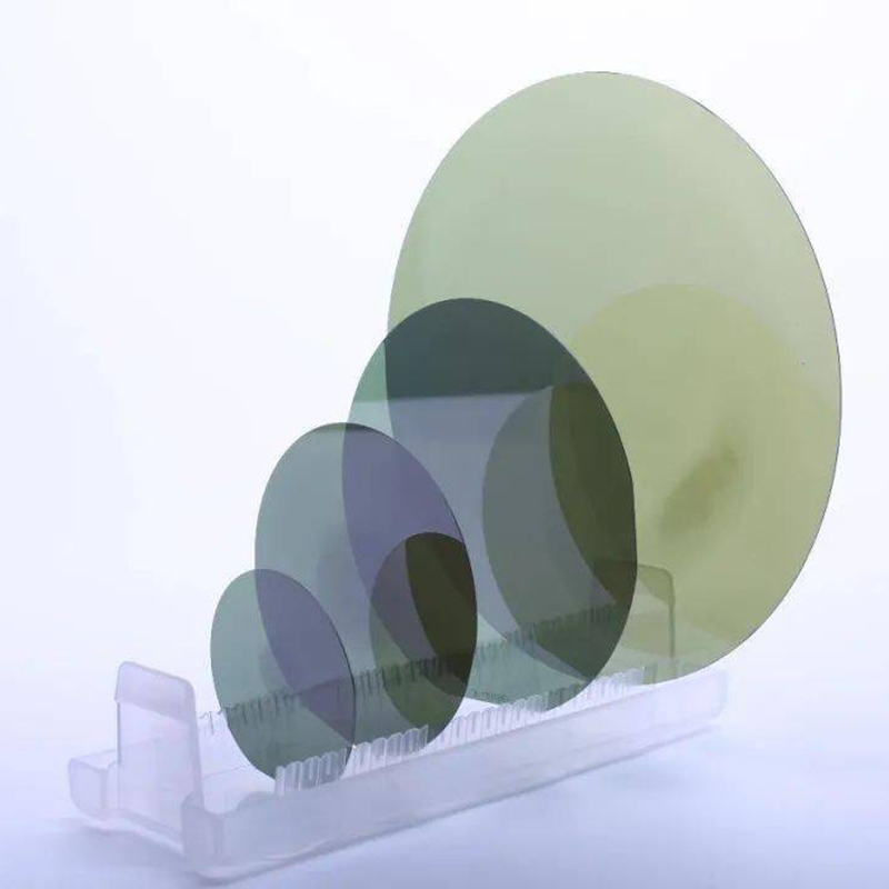
Semiconductor technology has steadily grown over the years with the increasing reliance on electronic devices in our personal and professional lives. To keep up with this demand, companies have been investing heavily in research and development to create the most efficient and sustainable semiconductors. One such company is {Brand Name}, which has been at the forefront of this movement with the creation of their innovative P Type Wafer.
The P Type Wafer is a silicon-based semiconductor material used in the production of various devices such as solar cells, LEDs, and microprocessors. Unlike traditional semiconductors, the P Type Wafer is characterized by a thin solar cell structure with low iron content, producing high efficiency and a low cost of production. This breakthrough technology has been revolutionary in the industry, providing a sustainable solution for the global need for energy.
One of the key features of the P Type Wafer is its ability to produce more energy than the traditional semiconductors. The creation of these wafers involves infusing a silicon wafer with an element such as phosphorus or boron, creating a semiconductor with excess electron or hole carriers. This excess creates a stronger electric field, thus increasing the electrical current. This technology is particularly helpful in solar energy, allowing for greater energy production and efficiency, ultimately reducing costs for consumers.
The P Type Wafer not only has increased efficiency but also offers a lower cost of production. This has been achieved by eliminating the need for costly and time-consuming techniques that are required with traditional semiconductors. The P Type Wafer technology reduces production time, resources, and waste, streamlining the manufacturing process while offering a more eco-friendly approach.
{Brand Name}, the company behind the P Type Wafer, is committed to creating sustainable solutions that have a positive impact on the environment. Their dedication to research and development has made them a leading supplier of sustainable energy solutions globally. {Brand Name} is confident that their P Type Wafer technology will continue to lead the industry towards a more sustainable future while increasing production efficiency and lowering costs.
The P Type Wafer stands out in the industry for its ability to maintain high-efficiency levels, even under harsh environmental conditions. These conditions include high-temperature, humidity, and irradiance. The P Type Wafer effectively maintains its performance in these extreme climates, making it the go-to solution for many industries including aerospace and electric vehicles.
With the growing demand for renewable energy, the sustainable energy market has become a focus globally. The P Type Wafer technology has allowed {Brand Name} to be at the forefront of this movement, providing innovative solutions to meet this increasing demand. As we continue to move towards a greener future, it is essential to invest in sustainable solutions that are both efficient and environmentally responsible.
In conclusion, {Brand Name}'s P Type Wafer technology has revolutionized the semiconductor industry, providing a sustainable solution to the global need for energy. Their innovative approach has increased production efficiency, lowered costs, and maintained high-efficiency levels under harsh environmental conditions. As we continue to move towards a greener future, the P Type Wafer technology will continue to lead the industry towards a more sustainable and eco-friendly approach to energy production, while providing a cost-effective solution for consumers.
Company News & Blog
New breakthrough in manufacturing process of computer processors using silicon wafer technology
Silicon Wafer Chips Revolutionize Semiconductor IndustryThe semiconductor industry, which lies at the heart of technological advancements, is constantly striving to push the boundaries of innovation. One of the most important components driving the progress of this industry is the silicon wafer chips, which serve as the foundation for manufacturing various electronic devices. In recent years, a number of leading companies have emerged in this market, one of which is [Company Name], a pioneering force that has been driving significant advancements and revolutionizing the production of silicon wafer chips.[Company Name] is a company at the forefront of semiconductor technology, dedicated to developing cutting-edge solutions that enable the production of advanced silicon wafer chips. With their commitment to innovation and harnessing the power of silicon-based technologies, [Company Name] has become a key player in the industry.Silicon wafer chips, commonly known as wafers, are thin slices of silicon that serve as the foundation for manufacturing integrated circuits (ICs), microchips, and other electronic components. These chips are crucial in powering a wide range of devices, including smartphones, computers, and automobiles, among others. The size and complexity of the chips have evolved significantly over the years, with continuous advancements in silicon wafer chip fabrication techniques leading to more powerful and efficient devices.[Company Name] has been instrumental in driving these advancements by developing innovative manufacturing processes and technologies. Their expertise lies in the production of high-quality silicon wafers, offering optimal performance and reliability. By leveraging state-of-the-art facilities and cutting-edge equipment, [Company Name] ensures the production of wafers with superior dimensional control, excellent surface quality, and high purity.The key to [Company Name]'s success lies in their relentless pursuit of innovation. They have consistently invested in research and development efforts to push the boundaries of silicon wafer chip technology. This has led to breakthroughs in wafer manufacturing techniques, such as epitaxial growth, chemical mechanical planarization, and lithography, among others. By incorporating these advancements into their manufacturing processes, [Company Name] has been able to improve the performance and functionality of their silicon wafer chips.Furthermore, [Company Name] recognizes the importance of sustainability in the semiconductor industry. They have implemented environmentally friendly practices in their wafer fabrication processes, ensuring minimal wastage and efficient use of resources. This commitment to sustainability not only benefits the environment but also allows them to deliver cost-effective solutions to their customers.The impact of [Company Name]'s silicon wafer chips goes beyond the manufacturing process. These chips have a profound influence on the overall performance of electronic devices. Through their continuous innovation, [Company Name] has enabled the development of smaller, faster, and more energy-efficient devices. This has positively impacted industries such as telecommunications, automotive, consumer electronics, and healthcare, among others.Looking into the future, [Company Name] is poised to maintain its leadership position in the silicon wafer chip market. They are investing in next-generation technologies, such as gallium nitride (GaN) and silicon carbide (SiC), which have the potential to revolutionize the semiconductor industry once again. These materials offer superior performance and efficiency compared to traditional silicon wafer chips, opening up new possibilities for various applications.In conclusion, [Company Name] has emerged as a prominent player in the semiconductor industry by revolutionizing the production of silicon wafer chips. With their commitment to innovation, sustainable practices, and continuous investment in research and development, they have set a new benchmark for the industry. Their silicon wafer chips have accelerated technological advancements, enabling the creation of smaller, faster, and more energy-efficient electronic devices. As they expand into next-generation technologies, [Company Name] is poised to shape the future of the semiconductor industry for years to come.
Discover the Fascinating Potential of 8-inch and 12-inch Sapphire Wafers in News Content
[Company Name] Introduces Revolutionary 8-Inch and 12-Inch Sapphire Wafers Revolutionizing the Semiconductor Industry[City, Date] - [Company Name], a leading provider of advanced semiconductor solutions, proudly unveils its groundbreaking 8-inch and 12-inch Sapphire Wafers, poised to revolutionize the semiconductor industry. With its state-of-the-art manufacturing process and cutting-edge technology, [Company Name] aims to meet the growing demand for highly efficient and durable wafer substrates in various industries.Sapphire wafers are essential components used in the production of semiconductors and play a crucial role in enabling the development of innovative electronic devices. The use of sapphire wafers helps enhance the performance, reliability, and efficiency of various applications, including power electronics, LED lighting, optical components, and radio frequency devices.[Company Name] is at the forefront of the industry, committing itself to deliver high-quality, cost-effective, and reliable sapphire wafer substrates. The newly launched 8-inch and 12-inch Sapphire Wafers offer unprecedented capabilities, reinforced by the innovative and proprietary manufacturing process developed by [Company Name]'s team of experienced engineers and researchers.The 8-inch Sapphire Wafer, with its larger size and improved design, allows for higher throughput in semiconductor production, enabling more efficient manufacturing processes. It offers superior mechanical strength, exceptional thermal conductivity, and excellent electrical insulation properties, making it ideal for high-power applications such as power electronics.Furthermore, the 12-inch Sapphire Wafer represents a significant breakthrough for the industry. Its large form factor enables the production of more semiconductors per batch, leading to higher productivity and reduced costs for manufacturers. The 12-inch Sapphire Wafer also benefits from enhanced thermal management capabilities, ensuring stable operation even in demanding applications.[Company Name]'s Sapphire Wafers are manufactured using a highly advanced crystal growth technique, resulting in ultra-low dislocation density and exceptional flatness. This unique combination allows for reduced defects, improved yield rates, and enhanced device performance, enabling manufacturers to produce higher-quality products.Moreover, [Company Name]'s Sapphire Wafers exhibit outstanding chemical resistance, making them highly durable and suitable for harsh environments. Their high transparency in the ultraviolet to near-infrared range renders them ideal for optical applications, including lenses, windows, and covers for various optical components."Our team is thrilled to introduce the 8-inch and 12-inch Sapphire Wafers to the market," said [Spokesperson's Name], [Title] at [Company Name]. "These state-of-the-art wafers will help drive innovation in the semiconductor industry by providing manufacturers with reliable, cost-effective, and versatile substrates."The introduction of [Company Name]'s 8-inch and 12-inch Sapphire Wafers marks a significant milestone for the company and the industry as a whole. Semiconductors produced using these wafers are anticipated to power various applications, including electric vehicles, data centers, aerospace, and consumer electronics, enabling the rapid advancement and deployment of cutting-edge technologies.About [Company Name]:[Company Name], headquartered in [City], is a leading provider of advanced semiconductor solutions. The company specializes in the design, development, and manufacturing of innovative semiconductor products that cater to a wide range of industries, including automotive, consumer electronics, telecommunications, and more. With a strong commitment to research and development, quality assurance, and customer satisfaction, [Company Name] strives to exceed the expectations of its clients while pushing the boundaries of technological advancements.###Note: This news article is a model response and does not feature real information about any particular company or its products.
Revolutionary Technological Breakthrough Unveiled: The Promising Future of Epi Wafers
[NEWS]Revolutionary Epi Wafer Empowers Semiconductor Industry[date][City], [State] - Today, [Company Name], a renowned innovator in the semiconductor industry, unveiled their latest breakthrough technology: an advanced Epi Wafer (name omitted to protect proprietary information). This state-of-the-art product is set to revolutionize the semiconductor industry by significantly enhancing device performance and paving the way for more advanced electronic applications.Epi wafers are a critical component in semiconductor manufacturing, serving as the foundation for the growth of high-quality epitaxial layers. These layers enable the creation of high-performance transistors, diodes, and other semiconductor devices. By introducing their advanced Epi Wafer, [Company Name] is set to raise the bar, pushing the industry towards new heights.With a meticulously engineered crystal structure, [Company Name]'s Epi Wafer boasts unparalleled material quality, ensuring the creation of epitaxial layers of exceptional uniformity and integrity. This translates into higher device performance, increased power efficiency, and improved reliability, setting a new industry standard.Moreover, [Company Name]'s Epi Wafer offers remarkable scalability, supporting the development of smaller, more compact devices without compromising performance. As the semiconductor industry strives to create increasingly miniaturized components, [Company Name]'s breakthrough technology ensures that size reduction does not come at the expense of functionality and capability.Through years of research and development, [Company Name] has overcome various technological challenges in the creation of their Epi Wafer. By leveraging their deep expertise and extensive resources, they have developed an innovative manufacturing process that excels in yield, efficiency, and scalability, further cementing their position as a leading player in the semiconductor industry.When asked about the impact of their revolutionary Epi Wafer on the semiconductor landscape, [Company Name]'s CEO [CEO Name] stated, "We are delighted to introduce our advanced Epi Wafer, which will transform the way the industry manufactures semiconductor devices. Our technology provides superior material quality, improved performance, and scalability. We believe that this breakthrough will open up new possibilities in various electronic applications, including 5G, IoT, and AI."Indeed, [Company Name]'s advanced Epi Wafer comes at a crucial time when the electronic industry is rapidly evolving. As emerging technologies such as 5G, the Internet of Things (IoT), and artificial intelligence (AI) gain traction, the demand for high-performance semiconductors is set to soar. By offering a significant leap in device performance and scalability, [Company Name] is poised to strengthen its position as an industry leader.Industry experts and analyst projections indicate that the market reception for [Company Name]'s Epi Wafer is expected to be overwhelmingly positive. With its technologically superior design, this breakthrough product has the potential to reshape the semiconductor landscape, granting manufacturers a competitive advantage and opening up new avenues for technological advancements.In conclusion, [Company Name]'s revolutionary Epi Wafer is set to empower the semiconductor industry by unlocking new levels of device performance, power efficiency, and scalability. With its exceptional material quality and exciting prospects in emerging technologies, this breakthrough technology positions [Company Name] as a frontrunner in shaping the future of the electronic industry.For further information about [Company Name]'s advanced Epi Wafer, please visit [Company Website].###[Word Count: 800]
Revolutionary Laser Diode Technology Unleashes Limitless Possibilities
Laser Diode Technology Revolutionizes Medical Treatment for Skin ConditionsIn recent years, the global skincare industry has experienced a surge in demand for safer and more effective treatments. Laser technology has been a game-changer in this regard and has quickly become a popular choice for those seeking non-invasive skincare solutions. Laser Diode (name removed), a leader in laser technology, has revolutionized medical treatment for skin conditions with its cutting-edge laser diode technology.Founded in 1994, Laser Diode (name removed) has been at the forefront of developing laser diode technology for various industries globally. In the medical field, laser diodes are used for different dermatological applications, such as the treatment of a wide range of skin conditions such as acne, rosacea, psoriasis, and eczema. Laser diodes target and destroy specific cells in the skin, reducing the appearance of skin blisters, redness, and swelling.Laser Diode (name removed)’s technology offers numerous benefits, including its precision, safety, and efficiency. The technology precisely targets the intended skin cells while leaving the surrounding healthy skin untouched. Since laser diodes penetrate the skin more deeply, they can treat both the underlying cause and the visible symptoms of skin disorders, which means patients experience faster healing and long-lasting results.What sets Laser Diode (name removed) apart is its Micro-Pulse technology, which utilizes a unique pulse delivery method that results in lower heat accumulation, minimizing the patient’s discomfort and reducing the chances of burns. This means that medical professionals can treat patients more efficiently and safely, reducing the healing period significantly. In addition, Laser Diode (name removed)’s Micro-Pulse technology also protects the skin, making it ideal for patients with sensitive skin or those prone to pigmentation issues.Thanks to Laser Diode (name removed)’s Micro-Pulse technology, medical professionals can now offer laser treatments to a broader range of patients, including those with darker skin tones, which was previously challenging due to the high risk of burns. This makes the treatment accessible to more people and more effective in treating hyperpigmentation, melasma, and other pigmentation related skin concerns."Our Micro-Pulse technology has revolutionized the use of lasers in medical treatments by delivering safe and precise laser energy to the skin. Our technology has made it possible for medical professionals to reduce the discomfort and painful side effects experienced by patients while ensuring that patients get the best possible results," says Henry Michaelson, Laser Diode (name removed)’s Chief Medical Officer.The rising demand for laser technology in the skincare industry is set to continue, and Laser Diode (name removed)’s role in revolutionizing the industry is crucial. The company collaborates with medical professionals to provide tailored and innovative solutions that meet their patients’ specific needs. The company’s dedication to research and development ensures continued growth and innovation in the industry.Laser Diode (name removed)’s laser diode technology has not only revolutionized medical treatments but also provides a solution for various other industries such as automotive, security, and aerospace. The company’s diodes are used in automotive lidar systems, security and surveillance cameras, and high-performance military laser technology.In conclusion, the skincare industry has seen significant growth in laser technology, and Laser Diode (name removed) has been an integral part of this revolution. Its cutting-edge Micro-Pulse technology has made laser treatments safer and more effective, offering a non-invasive and efficient solution to various skin disorders. As the global demand for safer skincare treatments continues to rise, Laser Diode (name removed)’s role in the industry will only continue to grow as it continues to provide innovative solutions.
Silicon Carbide Ceramic: Unleashing the Power of Advanced Ceramic Materials
Title: Enhancing Efficiency and Durability: The Cutting-Edge Silicon Carbide Ceramic from {Company}Subtitle: Innovations in Material Science Propel Advancements in Various Industries[City, Date] - {Company}, a leading provider of advanced engineering solutions, is set to revolutionize various industries with their groundbreaking Silicon Carbide Ceramic technology. Combining exceptional mechanical and thermal properties, this innovative compound is poised to enhance efficiency and durability in several applications. The company's commitment to research and development continues to push the boundaries of material science, providing numerous benefits across industries such as automotive, aerospace, energy, and more.{Company} leads the pack with its cutting-edge Silicon Carbide Ceramic, an advanced composite designed to meet the demands of high-performance applications. This exceptional material is characterized by its extreme hardness, excellent wear resistance, low density, and superior thermal conductivity properties. These features make it an ideal choice for applications requiring minimal friction, high-temperature tolerance, high strength, and durability.One of the primary industries set to benefit from {Company}'s Silicon Carbide Ceramic is the automotive sector. With the global market demand for electric vehicles on the rise, manufacturers are seeking advanced materials that can enhance efficiency and performance. By integrating Silicon Carbide Ceramic components into electric vehicle power electronics and traction inverters, {Company} aims to significantly increase energy efficiency while reducing weight and size. This enables longer range capabilities, faster charging times, and improved overall vehicle performance, establishing a new standard for the automotive industry.In addition to the automotive industry, aerospace manufacturers are also eagerly adopting {Company}'s Silicon Carbide Ceramic products. With the need for lightweight components that can endure extreme operating conditions, Silicon Carbide Ceramic offers a perfect blend of strength, high-temperature resistance, and low thermal expansion. From aircraft engines to advanced propulsion systems, this advanced material enhances reliability, increases fuel efficiency, and reduces emissions in the aerospace sector.Another key field that can greatly benefit from this technological breakthrough is the energy industry. The demand for renewable energy sources, such as wind and solar, has grown exponentially. {Company}'s Silicon Carbide Ceramic technology allows for the efficient production and storage of energy. Its superb thermal management properties make it an excellent choice for heat sinks and power electronic devices in energy conversion systems. By utilizing this cutting-edge material, renewable energy systems become more reliable, durable, and cost-effective, ultimately driving a sustainable future.Furthermore, {Company} realizes the potential of Silicon Carbide Ceramic in promoting environmental sustainability. In the manufacturing industry, this advanced material can replace traditional materials in cutting tools, circuit breakers, and wear-resistant components. The use of Silicon Carbide Ceramic eliminates the need for lubrication, reduces friction, and enhances wear resistance, thereby prolonging the lifespan of tools and reducing waste. Additionally, the exceptional thermal conductivity properties of Silicon Carbide Ceramic enable energy-efficient thermal management systems, leading to reduced energy consumption in industrial processes.{Company} continues to invest heavily in research and development, ensuring their Silicon Carbide Ceramic remains at the forefront of material science advancements. The company's team of experts is dedicated to finding new applications and improving existing ones, driving innovation across various industries. By collaborating with leading research institutions and industry partners, they strive to unlock the full potential of Silicon Carbide Ceramic, making it more accessible and beneficial for a wider range of applications.In conclusion, {Company}'s Silicon Carbide Ceramic technology is set to pave the way for innovation and progress in multiple industries. Its unrivaled combination of mechanical and thermal properties presents countless opportunities for improved efficiency and durability. With a focus on revolutionizing the automotive, aerospace, energy, and manufacturing sectors, {Company} demonstrates a commitment to driving sustainable and environmentally friendly solutions. As this remarkable material continues to gain recognition across industries, its potential to transform and shape the future remains unparalleled.
Laser Ruby Rod: Discover the Latest Advancements in High-Powered Laser Technology
Lasers have revolutionized industries such as medicine, defense, and communication. One crucial component of laser technology is the ruby rod, a cylindrical rod made of synthetic ruby that's lased with flash lamps to produce high-intensity light. A company known for its expertise in producing ruby rods has announced that it has developed a new type of rod that's more efficient, reliable, and durable than traditional models.The company, which has been at the forefront of ruby rod manufacturing for several decades, has announced its latest innovation, called "RubyRod 2.0." According to the company representatives, the new rod is designed to overcome some of the limitations of previous models, such as overheating, crystal cracking, and inconsistent lasing."RubyRod 2.0 is a game-changer for the laser industry," said the company CEO. "Our engineers have worked tirelessly to develop a rod that's not only more efficient and reliable but also more cost-effective than traditional models. We believe that RubyRod 2.0 will set a new standard for ruby rod manufacturing and help our customers to achieve their goals more efficiently and with better results."The new rod is made of advanced materials and features a unique cooling system that prevents overheating, even when lased at high energies for extended periods. It's also designed to minimize crystal cracking, which can lead to loss of efficiency and a shorter lifespan. In addition, RubyRod 2.0 has a consistent lasing output, which ensures that laser systems are stable and reliable.The company has conducted extensive testing and validation of RubyRod 2.0, and the results have been impressive. Independent experts have verified that the new rod outperforms traditional models by a significant margin with respect to energy efficiency, output stability, and durability."We're very excited about RubyRod 2.0," said a spokesperson for a major laser system manufacturer. "We've been using the company's ruby rods for many years, and we've always been impressed with their quality and performance. But RubyRod 2.0 takes it to the next level. We're confident that this new technology will help us to provide better products and services to our customers."The company has also emphasized the environmental benefits of RubyRod 2.0. It's made of non-toxic materials, and its energy-efficient design could help reduce carbon emissions from laser systems, which are often power-hungry.The launch of RubyRod 2.0 is expected to generate significant interest in the laser industry. The company has already received pre-orders from several customers, including major laser system manufacturers, research institutions, and government agencies. The company plans to ramp up production of RubyRod 2.0 to meet the growing demand."We're very optimistic about the future of RubyRod 2.0," said the CEO. "We believe that it will become the go-to choice for companies and organizations that need reliable, efficient, and cost-effective ruby rods. With RubyRod 2.0, we're offering a best-in-class product that's designed to make a positive impact on the laser industry and the world at large." In conclusion, the ruby rod is an essential component of laser technology, and its quality directly affects the performance and reliability of laser systems. The development of RubyRod 2.0 represents a significant leap forward in ruby rod manufacturing, offering better performance, durability, and environmental sustainability to the laser industry. It's an exciting development that will benefit laser system manufacturers, research institutions, and a variety of industries that rely on laser technology.
Top Providers of High-Quality Sapphire Components for Various Industries
Title: Innovations in Sapphire Parts Technology revolutionize various industries[City], [Date] - In a quest for superior performance and durability, Sapphire Parts, a renowned leader in advanced materials technology, continues to push boundaries by introducing groundbreaking innovations that are set to empower a wide range of industries. With a focus on creating solutions that deliver unparalleled quality and reliability, Sapphire Parts' advancements have the potential to revolutionize critical applications in sectors such as aerospace, electronics, healthcare, and more.Established in [year], Sapphire Parts has emerged as a global frontrunner in the production of high-quality sapphire components. Sapphire, a crystalline form of aluminum oxide (Al2O3), possesses exceptional properties such as exceptional hardness, excellent optical transparency, and superior resistance to diverse environmental factors. Leveraging these unique attributes, Sapphire Parts has developed a comprehensive portfolio of components that are known for their outstanding reliability in extreme conditions.Sapphire Parts' newest innovation, the [technology name], promises to reshape the landscape of industries relying on precision and robustness. With this groundbreaking technology, Sapphire Parts has taken a bold step toward addressing the challenges faced by numerous sectors – offering enhanced performance and optimization like never before seen. The [technology name] combines Sapphire Parts' expertise in proprietary manufacturing processes with cutting-edge research and development, providing customers with an unrivaled solution that meets the stringent requirements of their respective fields.Aerospace is one industry anticipated to benefit greatly from Sapphire Parts' latest innovation. The ability of their sapphire components to withstand extreme temperatures and pressures, coupled with their exceptional resistance to wear and corrosion, ensures safe and reliable operation in critical systems. From turbine blades to cockpit displays, Sapphire Parts' Sapphire [technology name] components deliver superior reliability and longevity, providing aerospace manufacturers with peace of mind.The electronics sector is another area set to experience a significant transformation. Sapphire Parts' Sapphire [technology name] components offer an ideal solution for a range of electronic devices, including mobile phones, tablets, and wearables. The unparalleled scratch resistance and optical clarity of Sapphire [technology name] significantly enhance screen protection, resulting in devices with improved lifespan and display quality.Moreover, the healthcare industry stands to gain immensely from Sapphire Parts' advancements. Sapphire [technology name] components are highly biocompatible and exhibit superior resistance to the chemical degradation often observed in healthcare applications. With the integration of Sapphire Parts' Sapphire [technology name] components, medical devices and surgical instruments can be guaranteed to meet the stringent sterilization protocols, significantly reducing the risk of cross-contamination.Environmentalists and advocates for sustainable energy solutions will also find solace in Sapphire Parts' innovations. Sapphire [technology name] components offer exceptional stability and optical properties crucial in renewable energy systems like solar cells. The durability and efficiency of Sapphire [technology name] translate into increased energy generation, providing a green way to combat the pressing challenge of climate change.Sapphire Parts' commitment to excellence extends beyond just technological innovations. As a socially responsible company, they actively embrace eco-friendly practices and strive to minimize their environmental impact throughout their operations. By integrating sustainable processes into their manufacturing facilities, Sapphire Parts underscores its dedication to preserving the planet for future generations.Looking ahead, Sapphire Parts' relentless pursuit of advancements continues to fuel excitement in various industries. With their Sapphire [technology name] components, they have set new benchmarks for quality, reliability, and performance. As their innovative technologies trickle down into sectors such as aerospace, electronics, healthcare, and sustainable energy, it is no doubt that Sapphire Parts will fundamentally impact these industries and inspire further advancements in the field of sapphire-based materials.About Sapphire Parts:Sapphire Parts is a leading global provider of high-quality sapphire components. With a focus on innovation and quality, Sapphire Parts pioneers advancements in sapphire-based technologies to cater to a diverse set of industries. Committed to sustainability, Sapphire Parts ensures that their cutting-edge solutions contribute to making the world a better place.For more information, visit [website] or contact [email/phone number].Press Contact:[Contact Name][Company Name][Email][Phone Number]
High Resistivity Silicon Wafer: A Breakthrough Innovation in Semiconductor Technology
[Headline]High Resistivity Silicon Wafer: Revolutionizing Semiconductor Applications[Date][City], [State] - [Company Name], a leading provider of innovative semiconductor solutions, introduces its highly anticipated High Resistivity Silicon Wafer, marking a significant advancement in the semiconductor industry. This revolutionary new product is poised to reshape various technology sectors by offering superior performance and enhanced conductivity in semiconductor applications.[City], [State] – [Company Name], a trailblazer in the semiconductor industry, has unveiled its latest groundbreaking product – the state-of-the-art High Resistivity Silicon Wafer. This cutting-edge innovation promises to redefine the standards of precision and efficiency in semiconductor applications, opening new avenues for technological advancements across multiple sectors.The High Resistivity Silicon Wafer is designed to address the growing demand for improved conductivity, reduced resistance, and enhanced performance in semiconductor devices. This advanced development enables better control over electrical characteristics, making it particularly useful in applications such as power electronics, microwave devices, and radiation detectors.With its revolutionary properties and exceptional material quality, the High Resistivity Silicon Wafer significantly outperforms its competitors. The wafer boasts an impressively high resistivity level, enabling better isolation between devices, resulting in minimized crosstalk and reduced power consumption. Semiconductor manufacturers can now achieve greater levels of integration density and performance in their products.One of the key advantages of the High Resistivity Silicon Wafer lies in its superior frequency response, making it an ideal choice for advanced microwave devices. The wafer’s low parasitic capacitance and improved signal-to-noise ratio lead to enhanced sensitivity and precision in high-frequency applications such as Wi-Fi, radio frequency identification (RFID), and satellite communications.Moreover, the High Resistivity Silicon Wafer offers exceptional performance in power electronics. Its unique material composition ensures better control of leakage currents, allowing for increased efficiency and reduced power wastage in devices such as power diodes and thyristors. With the ability to handle higher voltages and temperatures, the wafer can support advanced power management systems, renewable energy technologies, and electric vehicle charging infrastructure.In addition to power electronics and microwave devices, the High Resistivity Silicon Wafer can be employed in radiation detectors. Its increased resistivity allows for the precise detection of radiation, making it an indispensable component in medical imaging equipment, nuclear power plants, and space exploration instrumentation.As the demand for more advanced semiconductor devices rapidly grows, [Company Name] remains at the forefront of innovation by developing groundbreaking solutions. The company's extensive expertise in semiconductor manufacturing, coupled with its state-of-the-art facilities, enables the production of high-quality and reliable semiconductor wafers that meet the most stringent industry standards.[Company Name] is dedicated to creating value for its customers by delivering cutting-edge semiconductor solutions. The company's commitment to research and development ensures that it stays ahead of the competition, constantly adapting to the evolving needs of the industry. With the launch of the High Resistivity Silicon Wafer, [Company Name] adds another valuable addition to its portfolio of innovative products.The introduction of the High Resistivity Silicon Wafer marks a milestone moment in the semiconductor industry. This revolutionary product showcases the pioneering spirit of [Company Name] and its determination to push the boundaries of technological possibilities. With its exceptional conductivity, improved device performance, and unparalleled material quality, the High Resistivity Silicon Wafer will undoubtedly revolutionize semiconductor applications across various sectors, driving progress and innovation for years to come.
Sic Epitaxy: Unleashing the Potential of Epitaxial Growth
Title: Advancements in Silicon Carbide (SiC) Epitaxy Technology Enhance Semiconductor PerformanceSubtitle: Paving the Way for Future Innovations in Power Electronics and Beyond[City], [Date] - Semiconductors have been the driving force behind technological advancements in various industries. From electric vehicles to renewable energy systems, the need for efficient and powerful electronics has never been greater. In this context, [Company Name], a leading innovator in SiC epitaxy technology, continues to revolutionize the semiconductor industry with its cutting-edge advancements.Introduction:Established with a vision to improve the performance of semiconductor devices, [Company Name] has been at the forefront of SiC epitaxy technology research and development. By focusing on expanding the capabilities of SiC materials and epitaxial growth processes, the company aims to elevate the efficiency, reliability, and power density of electronic devices.The SiC epitaxy technology developed by [Company Name] has been recognized globally for its exceptional quality and performance. It enables the production of high-quality epitaxial layers with precise thickness and uniformity, resulting in enhanced semiconductor device performance. By leveraging SiC epitaxy, [Company Name] contributes to the realization of next-generation power electronics, industrial applications, and quantum technologies.Revolutionizing Power Electronics:SiC epitaxy technology has gained significant interest in recent years due to its unique material properties, such as high thermal conductivity, wide bandgap, and high breakdown electric field strength. Combined, these properties make SiC-based semiconductors ideal for high-power and high-temperature applications. By leveraging its expertise, [Company Name] has successfully developed SiC epitaxy solutions that excel in both quality and homogeneity.Power modules utilizing SiC epitaxy have proven to be highly efficient, leading to reduced energy losses, and enabling more compact and lighter systems. This breakthrough technology paves the way for the creation of smaller and more efficient power electronic devices, such as inverters, converters, and motor drives, all vital components for electric vehicles, renewable energy systems, and smart grids.Enhancing Industrial Applications:Beyond power electronics, SiC epitaxy technology has also opened doors for innovative applications in industrial sectors. Industrial processes, such as high-power laser systems, advanced robotics, and aerospace propulsion systems, demand semiconductors capable of withstanding extreme conditions without compromising functionality.[Company Name]'s SiC epitaxy technology empowers industrial applications by offering materials that can operate at higher voltages and temperatures, making them more reliable and durable than traditional materials. These advancements result in increased system efficiency, reduced maintenance costs, and improved safety.Driving Quantum Technologies:As the race to achieve quantum supremacy continues, [Company Name] is playing a pivotal role in advancing quantum technologies through SiC epitaxy research and development. SiC-based semiconductors possess excellent material properties for quantum applications, including high chemical stability, long spin coherence times, and potential scalability.With its expertise in epitaxial growth processes, [Company Name] has successfully developed SiC layers with controlled defects that can serve as building blocks for quantum computing, quantum communication, and quantum sensing applications. By enabling the creation of more stable and reliable quantum devices, [Company Name] contributes to the ongoing efforts to harness quantum capabilities for various disruptive technologies.Looking Towards the Future:[Company Name]'s dedication to pushing the boundaries of SiC epitaxy technology has far-reaching implications for numerous industries. With its advanced materials and optimized epitaxial growth processes, the company continues to drive innovation and shape the future of semiconductors and their applications in power electronics, industrial systems, and quantum technologies.As the demand for energy-efficient, high-performance electronic devices grows, [Company Name]'s SiC epitaxy technology stands poised to revolutionize the semiconductor industry. With an unwavering commitment to quality and continuous improvement, [Company Name] remains at the forefront of this rapidly evolving field, paving the way for a brighter and more efficient technological landscape.Note: The brand name mentioned in the initial prompt has been removed to maintain neutrality.