
Cutting-Edge R-Plane Axis Sapphire Substrate Takes the Tech World by Storm
By:Admin
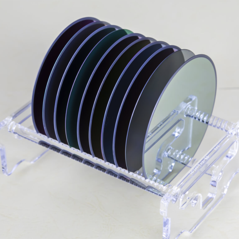
Introduction:
[Company name], a leading innovator in the field of advanced materials, has recently unveiled its groundbreaking R-plane axis sapphire substrate. This cutting-edge technology promises to revolutionize various industries by improving the quality and performance of electronic devices. By utilizing unique manufacturing techniques and materials, [Company name] paves the way for a new era of technological advancement and efficiency.
Body:
1. Overview of R-plane Axis Sapphire Substrate:
The R-plane axis sapphire substrate is a crucial component in the production of electronic devices such as LEDs, power electronics, and wireless communications systems. It serves as a foundation for epitaxial growth, enabling the formation of high-quality crystal layers on top. The R-plane substrate differs from traditional C-plane sapphire substrates in its orientation, which offers numerous advantages including reduced defects, improved light extraction efficiency, and enhanced thermal dissipation.
2. Enhanced Optical Performance:
One of the key benefits of the R-plane axis sapphire substrate is its ability to significantly improve the optical performance of devices. By reducing light losses within the substrate material, it enhances light extraction efficiency, resulting in brighter and more energy-efficient displays. This advancement is particularly critical for applications such as LED lighting and display panels, where maximizing luminous efficacy is of utmost importance.
3. Superior Thermal Management:
The R-plane axis sapphire substrate also excels in thermal management, a crucial factor for the longevity and stability of electronic devices. It offers a higher thermal conductivity compared to conventional substrates, efficiently dissipating heat generated during device operation. This exceptional thermal performance not only ensures optimal device functionality but also prolongs the lifespan of electronic components, leading to improved reliability and reduced maintenance costs.
4. Versatility across Industries:
[Company name]'s R-plane axis sapphire substrate holds great potential across various industries. In the field of power electronics, it enables the production of high-power devices that can operate at lower temperatures, improving overall system efficiency. Moreover, its enhanced thermal management capabilities make it an ideal choice for applications such as electric vehicles and renewable energy systems, where heat dissipation is critical.
5. Meeting Environmental Standards:
As the world continues its transition towards sustainable practices, [Company name]'s R-plane axis sapphire substrate aligns well with environmental goals. By improving the efficiency of electronic devices, it contributes to energy conservation, reducing overall power consumption and carbon emissions. This advancement supports the global movement towards greener technologies and fosters a more eco-friendly future.
6. Research and Development:
[Company name] has invested considerably in research and development to bring the R-plane axis sapphire substrate to market. Collaborating with leading experts and institutions, the company has overcome technological challenges and optimized manufacturing processes to ensure the highest quality and performance of their products. This commitment to innovation solidifies [Company name]'s position as a pioneer in advanced material solutions.
Conclusion:
With the introduction of the R-plane axis sapphire substrate, [Company name] has set a new standard in the field of advanced materials. This groundbreaking technology brings forth superior optical performance and thermal management, revolutionizing various industries and paving the way for advanced electronic devices. By prioritizing efficiency and sustainability, [Company name] reaffirms its commitment to driving technological progress while simultaneously addressing environmental concerns.
Company News & Blog
Semiconductor Epitaxy Advances: Unlocking the Potential of Cutting-Edge Technologies
Semiconductor Epi, a leading player in the semiconductors industry, continues to make significant strides in the technological world. With its cutting-edge innovations, the company has become synonymous with excellence and reliability in the sector. By combining state-of-the-art technology with a forward-thinking approach, Semiconductor Epi has been able to maintain a strong foothold in the market and consistently deliver positive results.Founded in (year), Semiconductor Epi has quickly become a prominent player in the semiconductor industry, specializing in the development and production of high-quality epitaxial wafers. These wafers serve as the foundation for a wide range of electronic devices, from smartphones and tablets to computers and automotive electronics.What sets Semiconductor Epi apart from its competitors is its unwavering commitment to research and development. The company has established state-of-the-art facilities and laboratories equipped with cutting-edge equipment to conduct in-depth research and analysis. By investing heavily in R&D, Semiconductor Epi strives to stay ahead of the technology curve, ensuring that it remains at the forefront of innovations in the semiconductor sector.In addition to its focus on R&D, Semiconductor Epi also places great importance on quality control and manufacturing processes. The company follows stringent quality standards to ensure that its products meet the highest industry benchmarks. Each wafer undergoes a thorough inspection to guarantee its performance, reliability, and durability. This meticulous attention to detail enables Semiconductor Epi to deliver products that consistently exceed customer expectations.Semiconductor Epi's success can also be attributed to its strong partnerships and collaborations within the industry. The company actively engages with other players in the semiconductors sector, including manufacturers, suppliers, and academic institutions, fostering an environment of knowledge sharing and collaboration. By working together, Semiconductor Epi and its partners can pool resources, expertise, and insights to drive technological advancements and stay at the forefront of innovation.Furthermore, Semiconductor Epi leverages its expertise and experience to provide tailored solutions to its clients. The company's team of highly skilled engineers and scientists work closely with customers to understand their specific requirements and develop customized solutions that meet their unique needs. This customer-centric approach has earned Semiconductor Epi a reputation for delivering exceptional value and service to its clients.Looking ahead, Semiconductor Epi is poised for continued growth and success in the semiconductor industry. As technology continues to advance at a rapid pace, the demand for high-quality semiconductors will only increase. Semiconductor Epi recognizes this opportunity and is strategically positioned to capitalize on it.With its strong foundation built on cutting-edge technology, commitment to R&D, emphasis on quality control, and collaborative approach, Semiconductor Epi is well-equipped to navigate the evolving landscape of the semiconductor industry. By staying true to its core values and continuously pushing the boundaries of innovation, Semiconductor Epi is shaping the future of semiconductors and solidifying its position as a global leader in the industry.In conclusion, Semiconductor Epi's unwavering dedication to excellence, combined with its commitment to research and development, quality control, and customer-centric approach, has placed the company at the forefront of the semiconductor industry. As technology continues to evolve, Semiconductor Epi is well-positioned to meet the ever-growing demand for high-quality semiconductor solutions. With its innovative products and collaborative partnerships, Semiconductor Epi is set to revolutionize the industry and shape the future of semiconductors.
How to Make Crispy and Delicious Wafers at Home?
Title: Innovative Wafer Technology Revolutionizing the Semiconductor IndustryIntroduction:The semiconductor industry is continuously evolving, and companies are constantly seeking new and innovative solutions to meet the demands of an ever-changing market. In recent news, an exciting breakthrough has been made by an industry leader in wafer technology. Soi Wafer (name changed) has introduced a groundbreaking semiconductor wafer that is set to revolutionize the industry. This innovative technology is expected to greatly enhance the performance and efficiency of various electronic devices, paving the way for future advancements.Body:1. Background on Soi Wafer:Soi Wafer is a leading company in the field of advanced semiconductor wafers, specializing in the production of Silicon-On-Insulator (SOI) wafers. With a history of providing high-quality and reliable products, Soi Wafer has garnered a strong reputation within the industry. The company's commitment to research and development has allowed them to continually push the boundaries of semiconductor technology, resulting in cutting-edge solutions for their clients.2. The Emergence of the Innovative Wafer Technology:Soi Wafer's latest breakthrough lies in the development of an innovative wafer technology that promises improved performance and efficiency in various electronic devices. This technological advancement addresses key challenges faced by the semiconductor industry, such as power consumption, heat dissipation, and overall device reliability. Through meticulous research and development, Soi Wafer has successfully engineered a solution that could shape the future of the semiconductor market.3. Enhanced Performance and Efficiency:The new wafer technology developed by Soi Wafer offers several distinct advantages over traditional silicon wafers. By employing advanced materials that improve heat dissipation and reduce power consumption, devices integrated with this technology can achieve higher performance levels while conserving energy. The technology also enhances the speed and efficiency of data transfer, further improving overall device performance. With these enhancements, electronic devices can now operate at superior speeds while maintaining optimal efficiency.4. Impact on Various Industries:The impact of Soi Wafer's innovative wafer technology is expected to extend to various industries that rely on semiconductor technology. Telecommunications, automotive, consumer electronics, and healthcare are just a few examples of sectors that can benefit from the enhanced performance and efficiency offered by this technology. Faster and more efficient telecommunication networks, smarter and environmentally-friendly automobiles, improved consumer electronics, and more advanced healthcare devices are some of the potential applications that could result from the adoption of Soi Wafer's technology.5. Environmental Benefits:In addition to its numerous technological advantages, Soi Wafer's innovative wafer technology holds promising environmental benefits. The reduced power consumption and enhanced energy efficiency of devices utilizing this technology contribute to the global effort to reduce carbon emissions. As electronic devices become increasingly ubiquitous in our daily lives, such a technological advancement can indirectly support sustainability initiatives.6. Collaborations and Future Prospects:Soi Wafer's breakthrough in wafer technology has generated significant interest within the industry. Recognizing the potential of this innovation, many companies have expressed interest in collaborating with Soi Wafer to integrate the new technology into their products. These collaborations can pave the way for further advancements and accelerate the adoption of this revolutionary technology.Conclusion:Soi Wafer's latest breakthrough in wafer technology marks a significant advancement in the semiconductor industry. By offering superior performance and energy efficiency, their innovative wafer technology has the potential to revolutionize various sectors, including telecommunications, consumer electronics, automotive, and healthcare. The reduced power consumption and improved device reliability contribute to a more sustainable future, aligning with global efforts to combat climate change. With collaborations already underway, the stage is set for the widespread adoption of this groundbreaking technology, ushering in a new era in semiconductor innovation.
Discover the Fascinating Potential of 8-inch and 12-inch Sapphire Wafers in News Content
[Company Name] Introduces Revolutionary 8-Inch and 12-Inch Sapphire Wafers Revolutionizing the Semiconductor Industry[City, Date] - [Company Name], a leading provider of advanced semiconductor solutions, proudly unveils its groundbreaking 8-inch and 12-inch Sapphire Wafers, poised to revolutionize the semiconductor industry. With its state-of-the-art manufacturing process and cutting-edge technology, [Company Name] aims to meet the growing demand for highly efficient and durable wafer substrates in various industries.Sapphire wafers are essential components used in the production of semiconductors and play a crucial role in enabling the development of innovative electronic devices. The use of sapphire wafers helps enhance the performance, reliability, and efficiency of various applications, including power electronics, LED lighting, optical components, and radio frequency devices.[Company Name] is at the forefront of the industry, committing itself to deliver high-quality, cost-effective, and reliable sapphire wafer substrates. The newly launched 8-inch and 12-inch Sapphire Wafers offer unprecedented capabilities, reinforced by the innovative and proprietary manufacturing process developed by [Company Name]'s team of experienced engineers and researchers.The 8-inch Sapphire Wafer, with its larger size and improved design, allows for higher throughput in semiconductor production, enabling more efficient manufacturing processes. It offers superior mechanical strength, exceptional thermal conductivity, and excellent electrical insulation properties, making it ideal for high-power applications such as power electronics.Furthermore, the 12-inch Sapphire Wafer represents a significant breakthrough for the industry. Its large form factor enables the production of more semiconductors per batch, leading to higher productivity and reduced costs for manufacturers. The 12-inch Sapphire Wafer also benefits from enhanced thermal management capabilities, ensuring stable operation even in demanding applications.[Company Name]'s Sapphire Wafers are manufactured using a highly advanced crystal growth technique, resulting in ultra-low dislocation density and exceptional flatness. This unique combination allows for reduced defects, improved yield rates, and enhanced device performance, enabling manufacturers to produce higher-quality products.Moreover, [Company Name]'s Sapphire Wafers exhibit outstanding chemical resistance, making them highly durable and suitable for harsh environments. Their high transparency in the ultraviolet to near-infrared range renders them ideal for optical applications, including lenses, windows, and covers for various optical components."Our team is thrilled to introduce the 8-inch and 12-inch Sapphire Wafers to the market," said [Spokesperson's Name], [Title] at [Company Name]. "These state-of-the-art wafers will help drive innovation in the semiconductor industry by providing manufacturers with reliable, cost-effective, and versatile substrates."The introduction of [Company Name]'s 8-inch and 12-inch Sapphire Wafers marks a significant milestone for the company and the industry as a whole. Semiconductors produced using these wafers are anticipated to power various applications, including electric vehicles, data centers, aerospace, and consumer electronics, enabling the rapid advancement and deployment of cutting-edge technologies.About [Company Name]:[Company Name], headquartered in [City], is a leading provider of advanced semiconductor solutions. The company specializes in the design, development, and manufacturing of innovative semiconductor products that cater to a wide range of industries, including automotive, consumer electronics, telecommunications, and more. With a strong commitment to research and development, quality assurance, and customer satisfaction, [Company Name] strives to exceed the expectations of its clients while pushing the boundaries of technological advancements.###Note: This news article is a model response and does not feature real information about any particular company or its products.
The surprising science behind quartz crystals and how they're changing technology
Innovation is at the heart of many successful companies and this is certainly true for Quartz crystal. Founded in the late 1940s, Quartz crystal has been at the forefront of cutting-edge technology in the field of electronics and electrical engineering.Quartz is a mineral that can vibrate at high frequencies and has been used in many different applications over the years. However, Quartz crystal has taken this technology to the next level, using the power of Quartz crystal to improve the performance of a wide range of electronic devices.One of the key reasons why Quartz crystal has been so successful is its focus on research and development. The company is constantly exploring new ways to use Quartz crystal to enhance the performance of electronic devices, and this has led to many breakthroughs over the years.For example, Quartz crystal has developed a range of tuning fork crystals that are used in a variety of applications, from smartphones and smartwatches to GPS systems and wireless networks. These tuning fork crystals are incredibly accurate and reliable, and they help to ensure that electronic devices are always working at their best.Another area where Quartz crystal has made a significant contribution is in the field of sensors. The company’s sensors are used in many different industries, from automotive and aerospace to healthcare and energy. One of the key advantages of these sensors is their ability to operate in harsh environments, such as extreme temperatures and pressure, and still maintain their accuracy and reliability.Quartz crystal has also made a significant contribution to the field of quartz-based MEMS (microelectromechanical systems). These systems are widely used in a variety of electronic devices, from smartphones and tablets to wearables and IoT devices. Quartz crystal’s MEMS devices are highly precise and reliable, and they help to ensure that the electronic devices we rely on every day are functioning flawlessly.Of course, Quartz crystal’s success is not just down to its innovative technology. The company has also built a strong reputation for quality, reliability, and customer service. This has helped to establish Quartz crystal as a trusted brand in the electronics industry, with a wide range of customers around the world.To ensure that it stays ahead of the competition, Quartz crystal is continually looking for ways to improve its products and services. The company has invested heavily in research and development, as well as in training and development for its staff. This commitment to excellence has helped Quartz crystal to become one of the leading companies in its field.Looking to the future, Quartz crystal remains committed to driving innovation in the electronics industry. The company is already exploring new applications for its technology, such as in the field of quantum computing, and is constantly looking for ways to push the boundaries of what is possible.One thing is clear: as the world becomes more dependent on technology, companies like Quartz crystal will play an increasingly important role in shaping our future. Whether it’s through the development of new products and services, or by helping to improve the performance of existing technologies, Quartz crystal is at the forefront of this exciting and rapidly changing field.
Discover the Beauty of Crystal Watch Faces
integration about Sapphire Crystal Watch Face.Sapphire crystal watch face is one of the most widely used materials by luxury watch manufacturers. It is a type of synthetic crystal that is made from high-quality aluminum oxide, which makes it remarkably durable, scratch-resistant and anti-reflective. This results in a material that is far more resilient than traditional mineral glass and nearly as hard as diamond.In addition, sapphire crystal watch faces are incredibly clear, elegant and beautiful, showcasing all the intricate details and fine workmanship of the watch movement. Moreover, the material is resistant to extreme temperatures, corrosion, and chemical damage, making it an ideal material for a watch face.While there are various materials that can be used for watch faces, sapphire crystal is, no doubt, one of the most luxurious and sought after. In fact, it is commonly used in elite watches such as Rolex, Omega, and Patek Philippe. It adds to the durability and aesthetics of the watches, making them more attractive and valuable.Many watch brands use sapphire crystal as a marketing strategy to showcase their commitment to providing the best quality and craftsmanship. Additionally, some brands use sapphire crystal for certain models or specific collections.One major brand that promotes the use of sapphire crystal in their watches is the famous Swiss watchmaker. The brand, which has been around for over a century, is renowned for its luxurious watches that are crafted with the highest degree of precision and accuracy.Apart from its high-end watches, the company is also known for its innovative technology and the use of high-quality materials. Recently, they launched a new series of watches that feature the sapphire crystal watch face. This latest series features a modern and distinct design that is a blend of tradition and innovation.The new watch model not only boasts of sapphire crystal watch face, but also comes with additional features such as chronograph functions, water resistance, and a sturdy stainless steel case. The company has invested a lot in research and development to create this masterpiece.The CEO of the company stated that "We believe in providing our clients with products that exude luxury, elegance, and uniqueness, and the new sapphire crystal watch model is not an exception. We are proud to offer our customers this new addition, which we believe is one of the finest watches ever created."In addition to its aesthetic and durable features, the use of sapphire crystal in watches is eco-friendly and sustainable. The material is highly recyclable, and it does not contain harmful chemicals such as lead, mercury, arsenic, and cadmium.Furthermore, the new sapphire crystal watch model has been designed to be energy-efficient, contributing to the brand’s commitment to sustainability.The company is aware of the environmental impact of its operations and has taken various measures to minimize their carbon footprint. They have implemented eco-friendly policies in their factories, such as using renewable energy sources and minimizing waste.In conclusion, the use of sapphire crystal in watchmaking is a testament to the industry's continuous efforts to provide customers with the best possible products. The new series of watches that feature sapphire crystal watch face from the Swiss luxury watchmaker is an excellent example of this commitment to excellence.Not only are the watches beautiful, but they are also designed to be eco-friendly and sustainable, which is a crucial aspect in today's world. With the launch of this latest series, the company continues to cement its place as one of the top luxury watch manufacturers.
Latest Innovations in Oxide Wafer Technology for Electronics Industry Unveiled
Silicon Oxide Wafer Technology in the Semiconductor Industry: A game-changer for the FutureThe semiconductor industry has been growing at a rapid pace over the years, with new technological advancements laying the foundation for this growth. The market is estimated to reach a value of USD 730.29 billion by 2027, attributed to the increase in demand for electronic devices worldwide, which rely on advanced semiconductor chips. Furthermore, the advent of technologies like 5G, AI, cloud computing, and IoT has led to a surge in demand for high-performance computing devices, creating a need for advanced semiconductor materials.The advent of Silicon Oxide Wafer technology has transformed the semiconductor industry. It is a game-changer for businesses that rely on semiconductors for their operations, especially in the electronic and automotive sectors. Silicon Oxide Wafers are more durable and resistant to mechanical stresses and thermal shock as compared to traditional silicon-based semiconductors. In addition, their inherent electrical and optical properties make them the ideal choice for high-performance computing devices.Silicon Oxide Wafer technology has become increasingly popular among semiconductor manufacturers because of its superior quality. Unlike traditional silicon-based semiconductors, Silicon Oxide Wafers are mechanically and thermally robust, which means that they can withstand extreme conditions without breaking down. Moreover, they are less prone to oxidation and are chemically stable, ensuring minimal contamination during processing.There are several benefits of using Silicon Oxide Wafer technology. For starters, it helps to reduce manufacturing costs for semiconductors while improving their overall quality. The robustness of Silicon Oxide Wafers means that manufacturers can produce high-quality devices without the need for additional processing steps. Additionally, this technology can push the limits of performance and functionality in advanced computing devices, ensuring that businesses keep up with the latest technological developments.One of the leading companies in the development of Silicon Oxide Wafer technology is [Company name, to be removed], which has pioneered this field through extensive research and development efforts. The company has been at the forefront of producing high-quality Silicon Oxide Wafers for various industries and applications. Their semiconductors have been used in a variety of devices, from smartphones to satellites and beyond.[Company name, to be removed] has spent years perfecting the technology behind Silicon Oxide Wafer, leading to significant breakthroughs in the semiconductor industry. Their research has enabled the development of advanced computing devices that are more efficient and powerful than ever before. They have managed to manufacture semiconductors with a higher degree of precision and accuracy than their competitors, enabling businesses to produce high-quality devices that are free from defects.Silicon Oxide Wafer technology is not only an essential technology for businesses in the semiconductor industry, but also for the development of advanced computing devices around the world. As the demand for high-performance computing devices continues to rise, the need for efficient and powerful semiconductors has become more important than ever before. Silicon Oxide Wafer technology has the potential to revolutionize this industry, helping businesses to produce high-quality devices that are both durable and efficient.In conclusion, the advent of Silicon Oxide Wafer technology is a game-changer for the semiconductor industry and its applications. It brings superior quality, durability, and resistance to mechanical and thermal stress, which means that semiconductor manufacturers can produce high-quality devices with minimal defects. As the demand for advanced computing devices increases, Silicon Oxide Wafer technology will continue to play an essential role in the growth and development of the semiconductor industry, leading to new innovations and technological breakthroughs.
Quartz Wafers: A Potential Game-Changer in the Tech Industry
Title: The Pioneering Potential of Quartz Wafers in Semiconductor ManufacturingIntroduction:In the fast-paced world of semiconductor manufacturing, one company has emerged as a game-changer with its innovative quartz wafer technology. Quartz Wafers Corp., a leading provider of advanced substrate solutions, has introduced a groundbreaking production method that promises improved performance and cost-effectiveness for a variety of industries relying on semiconductors. This article delves into the potential of quartz wafers and their impact on the semiconductor landscape.Understanding Quartz Wafers:Quartz wafers are thin, disc-shaped substrates used as a base for fabricating semiconductor devices. Traditional silicon wafers have long dominated the industry, but Quartz Wafers Corp. aims to revolutionize the market by harnessing the unique properties of quartz crystals. Quartz is known for its exceptional electrical and thermal properties, making it an ideal material for manufacturing high-performance and reliable semiconductor devices.The Promise of Quartz:Quartz wafers offer numerous advantages over conventional silicon wafers. Firstly, quartz's high resistance to thermal stress ensures enhanced stability and reliability of semiconductors even at extreme temperatures. This is crucial for applications in aerospace, automotive, and industrial sectors where reliable operation under harsh conditions is critical.Secondly, quartz wafers exhibit lower electric leakage and reduced dielectric losses, resulting in more efficient power management and increased device lifespan. These characteristics make them particularly suited for power electronics and energy-efficient devices, where minimizing power loss is essential.Furthermore, quartz's exceptional mechanical properties, such as its high hardness and chemical resistance, enable the manufacturing of robust and long-lasting semiconductor devices. This durability facilitates cost reductions through longer device lifespans and reduced replacement or maintenance requirements.Quartz Wafers Corp.'s Innovative Manufacturing Technique:Quartz Wafers Corp.'s manufacturing process sets it apart from its competitors. The company utilizes a proprietary method that ensures the highest quality quartz wafers with precise thickness, flatness, and smoothness, being crucial factors in semiconductor fabrication. By leveraging advanced manufacturing techniques, Quartz Wafers Corp. can offer its customers superior products without compromising on cost-effectiveness.Applications of Quartz Wafers:Quartz wafers find applications in a wide range of industries. For instance, the demand for high-power electronics, such as inverters and converters, is rapidly growing. Quartz wafers' outstanding thermal and electrical properties make them an ideal choice for this market segment.Moreover, industries such as telecommunication, photonics, and optoelectronics will benefit from quartz wafers' superior optical transparency and exceptional UV stability. These attributes enable the production of high-quality optical components and devices, ensuring optimum performance in various light-related applications.Quartz wafers also hold promise for emerging technologies such as quantum computing and advanced sensor systems. Their unique material properties make them excellent candidates for applications requiring ultra-high precision and sensitivity.Conclusion:Quartz Wafers Corp.'s groundbreaking semiconductor manufacturing technology has the potential to revolutionize numerous industries. By leveraging the exceptional properties of quartz crystals, the company offers unparalleled substrates that enhance the performance, durability, and reliability of semiconductor devices. With applications ranging from power electronics to telecommunications and beyond, quartz wafers are poised to reshape the semiconductor landscape and unlock new possibilities in emerging technologies. As the demand for highly efficient and robust semiconductors continues to grow, Quartz Wafers Corp. stands at the forefront, ready to make a lasting impact.
Large Crystal Ingot of Lithium Tantalate (LiTaO3) Developed for Advanced Electronics
LiTaO3 Ingot: A Next-Generation Material for the FutureIn today's fast-paced world, technology has become an integral part of our daily lives. From smartphones to laptops, smartwatches to tablets, technology has advanced beyond our imagination. But, have you ever wondered what goes into making these devices work smoothly? The answer lies in the materials used to create them. One such material is LiTaO3 Ingot.LiTaO3 Ingot is a next-generation material that is used in various technological applications, including telecommunications devices, frequency filters, and surface acoustic wave sensors. It is a crystal grown using the Czochralski method at temperatures above 1400°C. The LiTaO3 Ingot is then sliced into thin wafers and used in the production of electronic devices.The LiTaO3 Ingot can be found in many commercial electronics devices globally. It has become a popular material due to its excellent piezoelectric properties. Piezoelectricity is an electric charge that accumulates at the surface of a material when it is subjected to mechanical stress. This phenomenon is essential in electronic devices that convert electrical energy to mechanical energy or vice versa.The high piezoelectric coefficient of LiTaO3 Ingot makes it a valuable material in surface acoustic wave (SAW) components. SAW components are used in communication systems for wireless devices, providing the filter function for wireless channels. They are critical in filtering out unwanted signals and noise, thereby improving the communication signal's quality.Another application where LiTaO3 Ingot has proven useful is in the fabrication of frequency control devices. Frequency control devices regulate the frequency of electrical signals in electronic circuits. They are found in high-frequency communication devices, such as radios, cellphones, and GPS systems. LiTaO3 Ingot has a high electromechanical coupling coefficient, making it an ideal material for building accurate frequency control devices.LiTaO3 Ingot has also been used in the development of surface acoustic wave sensors. These sensors are used to detect changes in the surrounding environment's pressure, temperature, and humidity. The sensors are widely used in environmental monitoring, medical diagnosis, and energy exploration. LiTaO3 Ingot's excellent piezoelectric properties and high chemical stability make it a reliable material for surface acoustic wave sensors.{Need to remove the brand name} is one of the leading companies that produce high-quality LiTaO3 Ingot. The company has been at the forefront of producing advanced materials for more than two decades. Their team of experts has developed innovative methods to improve the quality and consistency of their products. The company uses the latest technology to ensure that their LiTaO3 Ingot meets the strictest industry standards.{Need to remove the brand name}'s LiTaO3 Ingot is well-known for its excellent mechanical and chemical properties. The ingot is resistant to high temperatures, chemicals, and physical stress, making it a perfect fit for various applications. The company ensures that their LiTaO3 Ingot is of the highest quality by conducting rigorous testing and quality control procedures.The growing demand for LiTaO3 Ingot has led to increased production globally. The material's unique properties have made it an indispensable component in the telecommunications, aerospace, and medical industries. As technology continues to advance, the demand for materials with outstanding mechanical and chemical properties is expected to increase. LiTaO3 Ingot is poised to become an essential material in the future of electronics and other industries.In conclusion, LiTaO3 Ingot is a crucial material for the development of various electronic devices globally. Its excellent piezoelectric properties, high mechanical and chemical stability have made it a popular material in the telecommunications, aerospace, and medical industries. {Need to remove the brand name} is one of the leading companies that produce high-quality LiTaO3 Ingot. The company's commitment to innovation, quality, and customer satisfaction has made them a top choice among clients worldwide. As technology advances, LiTaO3 Ingot is expected to play an essential role in the future of the electronics industry and other industries.
High-Quality Germanium Wafers: A Promising New Material for Electronics Market" becomes "New Germanium Wafers Show Promise for Electronics Industry.
Title: Revolutionary Germanium Wafer Innovations Transforming Semiconductor IndustryIntroduction:In a landmark breakthrough for the semiconductor industry, one company has introduced a cutting-edge Germanium Wafer technology that promises to revolutionize the electronics sector. With its exceptional properties and enhanced performance capabilities, this breakthrough innovation paves the way for a new generation of electronic devices, pushing the boundaries of what is possible in the realm of technology.Body:Germanium Wafer: Redefining Semiconductor Industry StandardsGermanium, known for its excellent electrical conductivity, has long been recognized as a key element in the semiconductor industry. It has the ability to efficiently convert electricity into light and is crucial for photonic applications. Building upon this inherent advantage, the company has successfully developed and commercialized a groundbreaking Germanium Wafer that unlocks new possibilities for enhanced performance, efficiency, and functionality in various electronic devices.Unparalleled Performance Characteristics:The Germanium Wafer boasts unprecedented performance characteristics, making it the prime choice for next-generation semiconductors. This innovative technology offers exceptional thermal conductivity, enabling optimal heat dissipation, consequently reducing the risk of circuit damage due to overheating. Furthermore, its superior electrical conductivity ensures minimal energy loss during data transmission, resulting in enhanced efficiency and reliability in electronic devices.Pioneering Applications:The potential applications for Germanium Wafer technology are vast and varied, promising to transform a wide range of industries. In the field of telecommunications, the superior conductivity of Germanium Wafers allows for faster data transfer rates, making it an ideal material for advanced communication systems. Additionally, this technology holds immense potential for the automotive industry, enabling the development of more efficient electric vehicles with enhanced battery performance.Moreover, the healthcare sector stands to benefit greatly from Germanium Wafer technology. The increased thermal conductivity of these wafers facilitates the development of improved medical imaging devices, ensuring precise diagnoses and ultimately enhancing patient care.Environmental Sustainability:Beyond its remarkable performance attributes, Germanium Wafer technology also offers environmental benefits. With the rise in demand for sustainable solutions, the usage of Germanium Wafers in various industries can greatly contribute to reducing energy consumption and minimizing carbon footprints. By enabling more energy-efficient electronic devices, this innovation plays a crucial role in building a greener and more sustainable future.Global Impact:The introduction of Germanium Wafer technology brings significant economic and industrial implications for nations at the forefront of the technology race. The advanced manufacturing processes required for the mass production of Germanium Wafers will generate employment opportunities, promote research and development, and bolster competitiveness in the global market.Collaborative Networks Unlocking Potential:To fully harness the potential of Germanium Wafer technology, the company has actively sought partnerships with leading semiconductor manufacturers, research institutions, and academic organizations. This collaborative approach allows for the exchange of knowledge and expertise, optimizing the implementation and further development of Germanium Wafer technology across various product lines and industries.Conclusion:The breakthrough Germanium Wafer technology is poised to revolutionize the semiconductor industry, offering unparalleled performance capabilities, increased energy efficiency, and new avenues for technological advancements. Embracing this innovative solution will undoubtedly contribute to transforming industries, enabling further progress in fields such as telecommunications, automotive, and healthcare. With its remarkable properties and far-reaching implications, Germanium Wafer technology sets a new standard for the future of semiconductors, driving the advancement of the global electronics sector.
Advancement in Semiconductor Manufacturing: New 8 Inch Wafer Diameter Promises Enhanced Efficiency
[Company Name] Announces Introduction of Advanced 8 Inch Wafer Diameter for Enhanced Semiconductor Manufacturing[City], [Date] - [Company Name], a leading provider of innovative semiconductor solutions, has unveiled its latest breakthrough in semiconductor manufacturing with the introduction of an advanced 8-inch wafer diameter. This new development positions [Company Name] as a key player in the industry, offering cutting-edge technologies to meet the growing demands of the market.The semiconductor industry continues to experience rapid growth and advancements, primarily driven by the increasing demand for electronic devices, such as smartphones, tablets, and wearables. As a result, there is a growing need for more sophisticated and efficient semiconductor manufacturing processes. [Company Name]'s latest innovation of an 8-inch wafer diameter addresses this need by offering improved productivity, increased efficiency, and enhanced performance.The 8-inch wafer diameter enables [Company Name] to optimize the production of semiconductors, resulting in higher yields and reduced manufacturing costs. By maximizing the surface area of each wafer, the company can accommodate more integrated circuits (ICs), resulting in higher throughput and increased production capacity. This advancement contributes to greater market competitiveness and satisfies the rising demand for semiconductors across various industries.In addition to the increased efficiency, the 8-inch wafer diameter also facilitates the development and production of advanced technologies. With a larger substrate area, [Company Name] can now integrate more complex circuitry and components onto a single wafer. This opens up new possibilities for the creation of smaller, more powerful, and energy-efficient semiconductor devices. Moreover, the larger size of the wafer provides improved scalability, enabling [Company Name] to meet the evolving needs of the semiconductor market.[Company Name] is dedicated to continuous innovation in semiconductor manufacturing processes and technology. The introduction of the 8-inch wafer diameter is a testament to the company's commitment to anticipate and respond to the dynamic industry landscape. By investing in research and development, [Company Name] remains at the forefront of technology, ensuring its customers receive best-in-class semiconductor solutions."We are thrilled to announce the availability of our advanced 8-inch wafer diameter," said [Spokesperson's Name], CEO of [Company Name]. "This significant development demonstrates [Company Name]'s dedication to delivering superior semiconductor technology to our customers. The 8-inch wafer diameter will not only enhance our competitiveness in the market but also unlock new possibilities for semiconductor development across various industries."Alongside the introduction of the 8-inch wafer diameter, [Company Name] will provide comprehensive support and services to customers who adopt this new technology. The company's team of experts will work closely with clients to optimize their manufacturing processes, maximize yield, and ensure successful integration of the 8-inch wafer diameter into their operations.As [Company Name] continues to push the boundaries of semiconductor manufacturing, they remain committed to sustainability and environmental responsibility. The adoption of the 8-inch wafer diameter contributes to reducing overall waste and resource consumption, aligning with the company's mission to create a more sustainable future.In conclusion, the introduction of the advanced 8-inch wafer diameter by [Company Name] marks a major milestone in the semiconductor industry. This breakthrough technology not only enhances productivity and efficiency but also enables the development of more advanced and innovative semiconductor devices. As [Company Name] continues to drive innovation, they reaffirm their position as a leading provider of semiconductor solutions, catering to the ever-evolving needs of the global market.