
Quality Science Laboratory Equipment for All Your Research Needs
By:Admin
The company offers a comprehensive range of laboratory equipment, including but not limited to, pipettes, centrifuges, microscopes, balances, and spectrophotometers. These instruments are essential for conducting various experiments and tests in fields such as biology, chemistry, physics, and environmental science.
Science Laboratory Equipment prides itself on delivering innovative and cutting-edge products that meet the evolving needs of modern laboratories. Its team of scientists and engineers is dedicated to developing and perfecting new technologies to enhance the efficiency and accuracy of laboratory processes.
In addition to its commitment to quality and innovation, Science Laboratory Equipment places a strong emphasis on customer satisfaction. The company offers personalized support and guidance to help customers select the right equipment for their specific applications. Furthermore, Science Laboratory Equipment provides comprehensive training and technical assistance to ensure that customers can maximize the performance of their instruments.
Recently, Science Laboratory Equipment unveiled its latest addition to its product line: a state-of-the-art spectrophotometer. This advanced instrument is designed to deliver exceptional performance and reliability, making it an invaluable tool for a wide range of scientific applications. With its user-friendly interface and powerful analytical capabilities, the new spectrophotometer is set to revolutionize the way laboratories conduct research and analysis.
The spectrophotometer boasts a number of features that set it apart from other instruments on the market. Its high-resolution optics and advanced light source technology ensure accurate and reproducible results, even for the most demanding applications. Furthermore, the spectrophotometer is equipped with a range of automated functions that streamline the analytical process, saving time and reducing the risk of human error.
One of the most exciting aspects of the new spectrophotometer is its compatibility with cloud-based data management systems. This feature allows users to seamlessly transfer and store their analytical data, enabling easy access and sharing across multiple devices and locations. Science Laboratory Equipment has also developed a dedicated mobile app that allows users to monitor and control the spectrophotometer remotely, providing unparalleled convenience and flexibility.
The launch of the new spectrophotometer represents Science Laboratory Equipment's ongoing commitment to advancing scientific research and analysis. By providing laboratories with the latest technological innovations, the company aims to empower researchers and analysts to achieve new breakthroughs and discoveries in their respective fields.
In addition to its product innovations, Science Laboratory Equipment continues to expand its global presence and reach. The company has established a strong network of distributors and partners around the world, enabling it to serve a diverse range of customers with varying needs and requirements. Science Laboratory Equipment also regularly participates in industry trade shows and exhibitions to showcase its products and connect with potential customers and collaborators.
Looking ahead, Science Laboratory Equipment is dedicated to furthering its mission of providing cutting-edge laboratory instruments and equipment to support scientific progress. The company's commitment to quality, innovation, and customer satisfaction positions it as a leading force in the scientific instrumentation industry, and it is poised to continue driving advancements in laboratory technology for years to come.
As the demand for high-quality laboratory equipment continues to grow, Science Laboratory Equipment stands ready to meet the needs of laboratories around the world. With its unparalleled expertise and dedication to excellence, the company is well-positioned to make a lasting impact on the scientific community and contribute to the advancement of knowledge and innovation.
Company News & Blog
Advanced Crystal Ingot Technologies Discovered for Enhanced Laser Applications
**Title: Groundbreaking YAG Crystal Ingot Revolutionizes the Semiconductor Industry***Date: [Insert Date]**Location: [Insert Location]**Introduction*In a groundbreaking development, a revolutionary YAG Crystal Ingot has emerged on the market, transforming the semiconductor industry. This high-performance crystal ingot, developed by [Company Name], promises to elevate the efficiency and functionality of electronic devices to unprecedented levels. With its exceptional properties, the YAG Crystal Ingot is poised to revolutionize various sectors, including telecommunications, consumer electronics, and even medicine.*Company Overview*[Company Name], a leading innovator in the field of advanced materials, has established itself as a pioneer in developing cutting-edge technologies. Focused on pushing the boundaries of what is possible, the company has constantly strived to develop solutions that address the evolving needs of industries globally. Their relentless pursuit of excellence has earned them a prominent position, with their products being used extensively across various sectors.*YAG Crystal Ingot: The Game Changer*The YAG Crystal Ingot, developed by [Company Name]'s team of brilliant scientists and engineers, has created a buzz in the semiconductor manufacturing domain. This crystal ingot is made from yttrium aluminum garnet, or YAG, which exhibits exceptional optical and thermal properties. The unique combination of these properties enables the YAG Crystal Ingot to outperform existing semiconductor materials in several key aspects.One of the most significant advantages of the YAG Crystal Ingot is its outstanding thermal conductivity. High thermal conductivity is essential in semiconductor applications, as it aids in efficiently dissipating heat generated during device operation. The YAG Crystal Ingot, thanks to its superior thermal conductivity, ensures that electronic devices can operate at higher power levels without the risk of overheating, ultimately boosting their performance and longevity.Additionally, the YAG Crystal Ingot's optical properties allow for enhanced light transmission, making it perfect for applications in optoelectronic devices such as lasers, LEDs, and optical amplifiers. Its ability to efficiently transmit light across a broad spectrum enables manufacturers to create more efficient and reliable devices, benefiting industries such as telecommunications, data centers, and medical diagnostics.Moreover, the YAG Crystal Ingot exhibits exceptional mechanical properties, offering superior resistance to shocks and vibrations. This resilience makes it an ideal material for manufacturing devices meant for rugged environments or those subjected to constant movement, such as aerospace and defense equipment.The outstanding performance of the YAG Crystal Ingot is a testament to [Company Name]'s commitment to advancing technology and delivering innovative solutions. Their investment in research and development has allowed them to overcome the limitations of traditional materials and introduce a game-changing semiconductor product.*Envisioning the Future*The implications of the YAG Crystal Ingot's development are profound and far-reaching. Industries that rely heavily on semiconductor technology, such as telecommunications, consumer electronics, automotive, and healthcare, will experience a paradigm shift with the integration of this advanced material.Telecommunications companies will benefit from the YAG Crystal Ingot's ability to enhance the overall efficiency and reliability of their networks. Faster data transfer, lower latency, and improved signal quality will improve the end-user experience and lay the groundwork for the future of connectivity.Consumer electronics will witness a new era of technological advancements, with devices that exhibit higher performance, improved energy efficiency, and longer lifespans. From smartphones to smart home devices, the integration of YAG Crystal Ingot will elevate the functionality and durability of these products, delighting consumers across the globe.The medical field will also embrace the YAG Crystal Ingot, as it offers groundbreaking opportunities for better diagnostic tools, advanced surgical equipment, and the development of innovative health monitoring devices. Improved precision, reliability, and safety will revolutionize patient care and enable medical professionals to achieve groundbreaking breakthroughs.*Conclusion*With the introduction of the YAG Crystal Ingot, [Company Name] has truly changed the game in the semiconductor industry. This remarkable crystal ingot's superior thermal conductivity, optical properties, and mechanical resilience make it an invaluable material for various applications. By leveraging the potential of the YAG Crystal Ingot, industries can elevate their performance, redefine technological norms, and ultimately shape a future that is brighter, faster, and more efficient than ever before.
P Type Wafer Production to Witness Significant Growth in the Semiconductor Industry
P Type Wafer Continues to Revolutionize the Semiconductor IndustrySemiconductor technology has steadily grown over the years with the increasing reliance on electronic devices in our personal and professional lives. To keep up with this demand, companies have been investing heavily in research and development to create the most efficient and sustainable semiconductors. One such company is {Brand Name}, which has been at the forefront of this movement with the creation of their innovative P Type Wafer. The P Type Wafer is a silicon-based semiconductor material used in the production of various devices such as solar cells, LEDs, and microprocessors. Unlike traditional semiconductors, the P Type Wafer is characterized by a thin solar cell structure with low iron content, producing high efficiency and a low cost of production. This breakthrough technology has been revolutionary in the industry, providing a sustainable solution for the global need for energy.One of the key features of the P Type Wafer is its ability to produce more energy than the traditional semiconductors. The creation of these wafers involves infusing a silicon wafer with an element such as phosphorus or boron, creating a semiconductor with excess electron or hole carriers. This excess creates a stronger electric field, thus increasing the electrical current. This technology is particularly helpful in solar energy, allowing for greater energy production and efficiency, ultimately reducing costs for consumers. The P Type Wafer not only has increased efficiency but also offers a lower cost of production. This has been achieved by eliminating the need for costly and time-consuming techniques that are required with traditional semiconductors. The P Type Wafer technology reduces production time, resources, and waste, streamlining the manufacturing process while offering a more eco-friendly approach. {Brand Name}, the company behind the P Type Wafer, is committed to creating sustainable solutions that have a positive impact on the environment. Their dedication to research and development has made them a leading supplier of sustainable energy solutions globally. {Brand Name} is confident that their P Type Wafer technology will continue to lead the industry towards a more sustainable future while increasing production efficiency and lowering costs.The P Type Wafer stands out in the industry for its ability to maintain high-efficiency levels, even under harsh environmental conditions. These conditions include high-temperature, humidity, and irradiance. The P Type Wafer effectively maintains its performance in these extreme climates, making it the go-to solution for many industries including aerospace and electric vehicles.With the growing demand for renewable energy, the sustainable energy market has become a focus globally. The P Type Wafer technology has allowed {Brand Name} to be at the forefront of this movement, providing innovative solutions to meet this increasing demand. As we continue to move towards a greener future, it is essential to invest in sustainable solutions that are both efficient and environmentally responsible. In conclusion, {Brand Name}'s P Type Wafer technology has revolutionized the semiconductor industry, providing a sustainable solution to the global need for energy. Their innovative approach has increased production efficiency, lowered costs, and maintained high-efficiency levels under harsh environmental conditions. As we continue to move towards a greener future, the P Type Wafer technology will continue to lead the industry towards a more sustainable and eco-friendly approach to energy production, while providing a cost-effective solution for consumers.
Sapphire Wafers: The Latest in Silicon Technology
Silicon On Sapphire Wafers (SOS) are becoming a popular choice for semiconductor manufacturers due to their superior performance and reliability. These wafers are made by depositing a thin layer of silicon on top of a sapphire substrate, resulting in a high-quality material that is ideal for a wide range of applications.One company that is at the forefront of SOS wafer production is {} (company name removed). With over 20 years of experience in the semiconductor industry, {} is a leading supplier of SOS wafers for customers around the world. The company's commitment to quality and innovation has made them a trusted partner for many semiconductor manufacturers."{} is dedicated to providing our customers with the highest quality SOS wafers that meet their exact specifications," said a spokesperson for the company. "We understand the unique requirements of the semiconductor industry and work closely with our clients to develop customized solutions that exceed their expectations."The superior performance of SOS wafers can be attributed to the combination of silicon and sapphire, which results in a material that offers excellent electrical, thermal, and mechanical properties. This makes SOS wafers ideal for a wide range of applications, including radio-frequency (RF) devices, power amplifiers, and high-temperature electronics.One of the key advantages of SOS wafers is their high isolation and low capacitance, which makes them ideal for RF applications. These wafers also offer excellent thermal conductivity, allowing them to dissipate heat more effectively than traditional silicon substrates. Additionally, the mechanical strength of sapphire makes SOS wafers more durable and resistant to damage, resulting in a longer lifespan for electronic devices.Another important factor driving the adoption of SOS wafers is their compatibility with industry-standard semiconductor fabrication processes. This allows semiconductor manufacturers to easily integrate SOS wafers into their existing production lines, minimizing the need for costly equipment upgrades.In addition to their superior performance and compatibility, SOS wafers also offer a number of environmental benefits. The use of sapphire, which is a naturally occurring material, reduces the environmental impact of semiconductor production. Additionally, SOS wafers have a longer lifespan than traditional silicon substrates, reducing the amount of electronic waste generated over time.As the demand for high-performance semiconductor devices continues to grow, the market for SOS wafers is expected to expand significantly in the coming years. {} is well-positioned to meet this growing demand, with the expertise and capabilities to deliver high-quality SOS wafers to customers worldwide."We are excited about the potential for SOS wafers to drive innovation and advancement in the semiconductor industry," said the spokesperson for {}. "With our proven track record and commitment to excellence, we are confident that {} will continue to be a leader in the production of SOS wafers for many years to come."In conclusion, Silicon On Sapphire wafers are emerging as a preferred substrate for semiconductor manufacturers due to their superior performance, reliability, and compatibility with industry-standard fabrication processes. As a leading supplier of SOS wafers, {} is well-positioned to capitalize on the increasing demand for this innovative material and drive further advancements in the semiconductor industry.
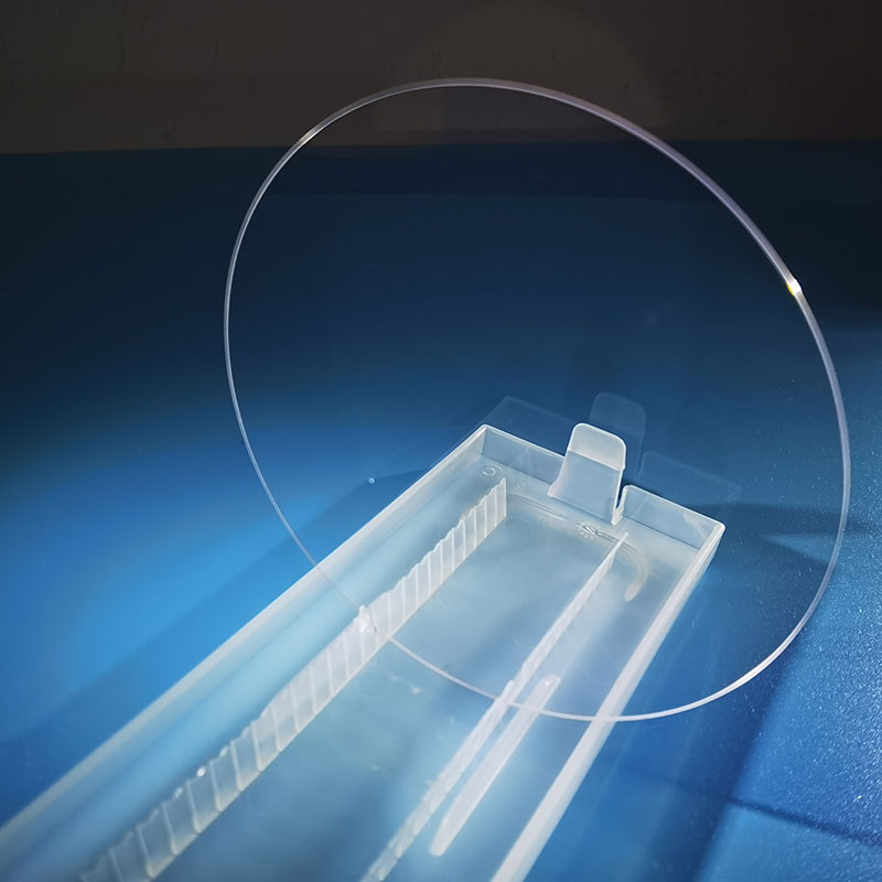
A Guide to M-Plane Axis Sapphire Substrate for High-Performance Electronics
M-Plane Axis Sapphire Substrate Revolutionizes Technology IndustryIn a groundbreaking development, an innovative company, referred to as "Company X" (for confidentiality purposes), has introduced a cutting-edge M-Plane Axis Sapphire Substrate. This remarkable invention is set to revolutionize the technology industry, enabling more efficient and effective manufacturing processes for various electronic devices.The M-Plane Axis Sapphire Substrate is a thin, transparent crystalline material that acts as a foundation for the production of advanced electronic devices like LEDs, lasers, and power electronics. With its unique properties, this substrate offers significant advantages over traditional silicon-based substrates, promising superior performance and enhanced durability.One of the key benefits of the M-Plane Axis Sapphire Substrate is its exceptional heat dissipation properties. Electronic devices often generate heat during operation, leading to performance degradation and even failure. By utilizing this advanced substrate, manufacturers can effectively manage heat dissipation, thereby ensuring the longevity and reliability of their products.Additionally, the M-Plane Axis Sapphire Substrate offers exceptional electrical insulation characteristics. This quality is crucial for electronic devices, as it prevents unwanted electrical leakage and interference, ensuring optimal performance. With this substrate, manufacturers can produce devices that operate flawlessly, even in high-stress environments.Furthermore, this revolutionary substrate provides superior optical properties compared to traditional alternatives. Its crystal structure enables efficient light transmission, making it ideal for applications such as LEDs and lasers. As a result, devices utilizing the M-Plane Axis Sapphire Substrate can achieve higher brightness, better color rendering, and improved overall performance.The development of the M-Plane Axis Sapphire Substrate marks a significant advancement in the technology industry, as it offers a wide range of applications. LED displays and lighting systems, for instance, can greatly benefit from the exceptional light transmission properties of this substrate, leading to clearer and more vibrant visuals.Moreover, power electronics, such as power converters and inverters, can profit from its superior heat dissipation capabilities. By incorporating the M-Plane Axis Sapphire Substrate into these devices, manufacturers can ensure their efficient operation, reducing energy loss and enhancing overall reliability.Company X, the mastermind behind this groundbreaking invention, is dedicated to providing high-quality products and advancing technological innovation. With cutting-edge research facilities and a team of exceptional scientists and engineers, they strive to push the boundaries of what is possible in the technology sector.Recognizing the tremendous potential of the M-Plane Axis Sapphire Substrate, Company X has invested substantial resources into developing a state-of-the-art manufacturing process. This ensures the production of substrates that adhere to strict quality standards, allowing their customers to benefit from the exceptional properties of this innovative material.The introduction of the M-Plane Axis Sapphire Substrate could not have come at a better time, as the technology industry constantly seeks advancements to meet the growing demands of consumers. This revolutionary substrate promises to elevate the performance, durability, and overall user experience of various electronic devices, ushering in a new era of innovation.In conclusion, the M-Plane Axis Sapphire Substrate developed by Company X represents a significant breakthrough in the technology industry. With its exceptional heat dissipation, electrical insulation, and optical properties, this revolutionary substrate offers clear advantages over traditional alternatives. As manufacturers begin to incorporate this advanced material into their products, we can expect a new wave of electronic devices that are more efficient, reliable, and visually appealing.
6-Inch Sapphire Wafer: Latest Advancements in Semiconductor Technology
The use of 6-inch sapphire wafers has been a game-changer in the semiconductor industry, as it has allowed companies to produce smaller and more powerful electronics. The demand for these wafers has been steadily increasing, and one company that has been at the forefront of this trend is {Company Name}.{Company Name} is a leading manufacturer of sapphire wafers, specializing in the production of 6-inch wafers that are used in a wide range of applications, including LED production, power electronics, and RF devices. The company has been in the industry for over a decade and has established itself as a reliable and innovative supplier of high-quality sapphire wafers.The use of 6-inch sapphire wafers has several advantages over smaller wafer sizes. First, larger wafers allow for greater economies of scale, resulting in lower production costs and higher yields. This is particularly important in the semiconductor industry, where margins are often tight, and any cost savings can have a significant impact on a company's bottom line.Additionally, the use of 6-inch wafers allows for the production of more chips per wafer, resulting in higher throughput and improved efficiency. This is crucial in meeting the increasing demand for smaller and more powerful electronic devices, as it allows manufacturers to produce more chips in a shorter amount of time.Furthermore, the larger surface area of 6-inch wafers provides greater flexibility in the design and layout of electronic components, allowing for more complex and integrated circuits to be produced. This is essential in meeting the ever-growing demand for advanced electronics that are smaller, faster, and more powerful.{Company Name} has been at the forefront of the 6-inch sapphire wafer market, providing its customers with high-quality wafers that meet the stringent requirements of the semiconductor industry. The company's wafers are known for their high crystal quality, low defect density, and excellent uniformity, making them the preferred choice for many leading semiconductor manufacturers.In addition to its superior product quality, {Company Name} prides itself on its exceptional customer service and technical support. The company works closely with its customers to understand their specific needs and requirements, and to provide them with tailored solutions that meet their exact specifications. This customer-centric approach has allowed the company to build strong and lasting partnerships with its customers, fostering trust and loyalty within the industry.Looking ahead, {Company Name} is committed to further advancing the 6-inch sapphire wafer technology, with a focus on improving crystal quality, reducing defect density, and enhancing overall wafer performance. The company is also investing in research and development efforts to explore new applications and opportunities for 6-inch sapphire wafers, in order to stay ahead of the curve and meet the evolving needs of the semiconductor industry.In conclusion, the use of 6-inch sapphire wafers has revolutionized the semiconductor industry, and {Company Name} has been at the forefront of this trend, providing high-quality wafers and exceptional customer service. As the demand for smaller and more powerful electronics continues to grow, {Company Name} is well-positioned to meet the needs of its customers and drive innovation in the industry.
Semiconductor Company Announces Breakthrough Technology in Latest News
Inp Semiconductor, a leading semiconductor manufacturer, has recently announced significant advancements in its production capabilities. The company has been a key player in the semiconductor industry for many years, consistently delivering high-quality products to its customers worldwide.Inp Semiconductor’s dedication to research and development has led to groundbreaking innovations in the semiconductor field. The company has continually invested in state-of-the-art technology and equipment to ensure that its products meet the highest industry standards. This commitment has positioned Inp Semiconductor as a trusted and reliable partner for businesses across various sectors, including telecommunications, automotive, consumer electronics, and more.With its recent advancements in production capabilities, Inp Semiconductor has demonstrated its commitment to meeting the growing demand for high-performance semiconductor solutions. The company's expanded manufacturing capacity will enable it to fulfill larger orders and deliver products to its customers in a more timely manner. This development is particularly significant given the current global semiconductor shortage, as it will allow Inp Semiconductor to play a crucial role in alleviating supply chain issues.In addition to expanding its production capabilities, Inp Semiconductor has also focused on enhancing its sustainability efforts. The company has implemented environmentally friendly practices in its manufacturing processes, reducing its carbon footprint and contributing to a greener future. This commitment to sustainability sets Inp Semiconductor apart as a socially responsible and forward-thinking organization in the semiconductor industry.Furthermore, Inp Semiconductor's dedication to innovation has led to the development of new and improved semiconductor products. The company's research and development team has been working tirelessly to create cutting-edge solutions that meet the evolving needs of its customers. Whether it's developing more energy-efficient chips or enhancing the performance of existing products, Inp Semiconductor is committed to staying at the forefront of technological advancements.Inp Semiconductor's success can be attributed to its strong focus on customer satisfaction. The company prioritizes building long-lasting relationships with its clients, understanding their unique requirements, and delivering tailor-made solutions. This customer-centric approach has earned Inp Semiconductor a reputation for reliability and excellence in the semiconductor industry.With its recent advancements in production capabilities and ongoing commitment to innovation and sustainability, Inp Semiconductor is poised for continued success in the semiconductor market. The company's dedication to meeting the needs of its customers, while also contributing to a more sustainable future, sets it apart as a leader in the industry.As the global demand for semiconductor products continues to rise, Inp Semiconductor's expanded production capabilities will enable the company to meet the growing needs of its customers. With a focus on innovation, sustainability, and customer satisfaction, Inp Semiconductor is well-positioned to remain a key player in the semiconductor industry for many years to come.
Latest News on Semiconductor Wafers: Valuable Insights on Industry Trends and Market Analysis
Title: Silicon Wafer Manufacturer, Inp Wafers, Revolutionizes Semiconductor IndustryIntroduction:Inp Wafers, a leading global manufacturer of high-quality silicon wafers, is reshaping the semiconductor industry with its advanced production techniques and unparalleled product offerings. The company prides itself on delivering cutting-edge solutions to meet the growing demands of the technology sector. Inp Wafers has now unveiled a groundbreaking innovation that promises to further enhance the performance and efficiency of electronic devices. This article explores the recent breakthrough by Inp Wafers, highlighting the potential impact it will have on the semiconductor industry.Body:1. The Importance of Silicon Wafers in Semiconductor Manufacturing:Silicon wafers serve as the foundational material in the production of semiconductors, which are vital components of various electronic devices. These wafers provide the surface where microchips and integrated circuits are built, enabling the creation of smaller, faster, and more powerful electronics. As the demand for high-performing electronic devices continues to surge, manufacturers like Inp Wafers play a crucial role in ensuring the supply of top-quality silicon wafers.2. Inp Wafers Introduces Advanced Manufacturing Technique:In its quest to push the boundaries of semiconductor technology, Inp Wafers has developed an innovative manufacturing technique that promises significant improvements in the efficiency and performance of electronic devices. The company has invested substantial resources in research and development to perfect this groundbreaking method, which combines precision engineering and state-of-the-art materials to create unparalleled silicon wafers.3. Enhanced Performance: The Advantages of Inp Wafers' Innovative Approach:Inp Wafers' advanced manufacturing technique enhances the performance capabilities of silicon wafers, resulting in superior electronic devices. These wafers exhibit remarkably low defect densities, ensuring consistently high yields during the semiconductor fabrication process. Moreover, Inp Wafers' innovative method allows for increased wafer thickness uniformity, enabling manufacturers to achieve precise control over device features. The improved uniformity also enhances transistor performance and reduces power consumption, supporting energy-efficient designs.4. Enhanced Product Offerings: Catering to Diverse Semiconductor Needs:Inp Wafers understands the diverse requirements of its customers and has developed an extensive product range to address specific industry demands. From standard silicon wafers to specialty wafers with unique properties, Inp Wafers offers a comprehensive portfolio to support various semiconductor applications. By providing tailored solutions for different industries, the company ensures that its customers have access to the most appropriate silicon wafers for their specific requirements.5. Partnering for Success: Collaborative Approach:Inp Wafers actively collaborates with leading semiconductor manufacturers, research institutions, and universities to foster innovation and create a vibrant ecosystem. The company recognizes the value of partnerships and invests in collaborative projects to leverage expertise and drive technological advancements. This collaborative approach strengthens the semiconductor industry as a whole, benefiting customers, stakeholders, and end-users alike.6. Sustainable Practices: Inp Wafers' Commitment to the Environment:Inp Wafers is committed to conducting business in an environmentally responsible manner. The company prioritizes sustainable production practices, ensuring minimal waste generation and emissions. With a focus on reducing its carbon footprint, Inp Wafers invests in clean energy alternatives and actively promotes recycling initiatives. By adopting these sustainable practices, the company aligns itself with global efforts to combat climate change and promote a greener future.Conclusion:Inp Wafers, a leading silicon wafer manufacturer, continues to redefine the semiconductor industry through its advanced manufacturing techniques and commitment to innovation. With its groundbreaking approach, Inp Wafers has elevated the performance capabilities of silicon wafers, contributing to the production of faster, smaller, and more energy-efficient electronic devices. As the demand for advanced semiconductors intensifies, Inp Wafers stands at the forefront of providing customized solutions to cater to diverse industry needs. With a collaborative approach and a strong focus on sustainability, Inp Wafers reinforces its commitment to shaping the future of the semiconductor industry.
High-Quality Crystal Substrate for Various Industries
Gsgg Crystal Substrate Breakthrough: A Game-Changer in Semiconductor IndustryIn a groundbreaking development, a leading semiconductor company has introduced a new Gsgg crystal substrate, which is set to revolutionize the semiconductor industry. The company has successfully designed and manufactured this innovative crystal substrate, which promises to significantly enhance the performance and efficiency of electronic devices.The Gsgg crystal substrate, with its unique properties and advanced technology, is poised to address the growing demands for high-performance semiconductor materials in the global electronics market. Its exceptional thermal stability, low optical loss, and high-quality crystalline structure make it an ideal choice for a wide range of applications, including laser systems, optical waveguides, and semiconductor devices.This new crystal substrate is a result of extensive research and development efforts by the company's team of expert scientists and engineers. Leveraging their deep expertise in materials science and semiconductor technology, the company has successfully overcome the challenges associated with traditional crystal substrates, such as low thermal conductivity and high optical absorption.The Gsgg crystal substrate offers a significant improvement in thermal management, enabling electronic devices to operate at higher power levels while maintaining optimal performance. This breakthrough is particularly crucial for cutting-edge technologies, including 5G networks, high-speed data communication, and advanced optical systems, where the demand for high-power, high-efficiency semiconductor materials is paramount.Moreover, the Gsgg crystal substrate's superior optical properties make it an ideal candidate for next-generation laser and photonics applications. Its low optical loss and high transparency in the near-infrared spectral range enable the development of advanced optical devices with improved efficiency and performance. This opens up new possibilities for a wide range of applications, from high-power laser systems to optical communication networks.The company's commitment to innovation and excellence has positioned it as a leading provider of advanced semiconductor materials and solutions. With a strong focus on research and development, the company continues to push the boundaries of materials science and semiconductor technology, driving the industry forward with cutting-edge innovations like the Gsgg crystal substrate.Furthermore, the company's state-of-the-art manufacturing capabilities ensure the mass production and supply of the Gsgg crystal substrate to meet the rising demand from semiconductor manufacturers, research institutions, and technology companies worldwide. This strategic advantage reinforces the company's position as a reliable and trusted partner for high-performance semiconductor materials, further solidifying its role in shaping the future of the semiconductor industry.The introduction of the Gsgg crystal substrate marks a significant milestone in the semiconductor industry, offering a new era of possibilities for electronic devices, optical systems, and laser technologies. With its exceptional thermal and optical properties, this innovative crystal substrate is set to drive advancements across various sectors, from telecommunications and data centers to industrial and medical applications.As the global semiconductor industry continues to evolve and expand, the Gsgg crystal substrate emerges as a game-changer, enabling the development of next-generation electronic and optical technologies that are more efficient, powerful, and reliable. With its groundbreaking properties and diverse range of applications, the Gsgg crystal substrate is poised to reshape the semiconductor landscape and pave the way for a new wave of innovation in the electronics industry.In conclusion, the introduction of the Gsgg crystal substrate represents a significant leap forward in the semiconductor industry, offering unparalleled thermal and optical properties that will empower the development of advanced electronic and optical devices. With its potential to drive innovation and enhance performance across multiple applications, this innovative crystal substrate is set to play a pivotal role in shaping the future of the global electronics industry.