
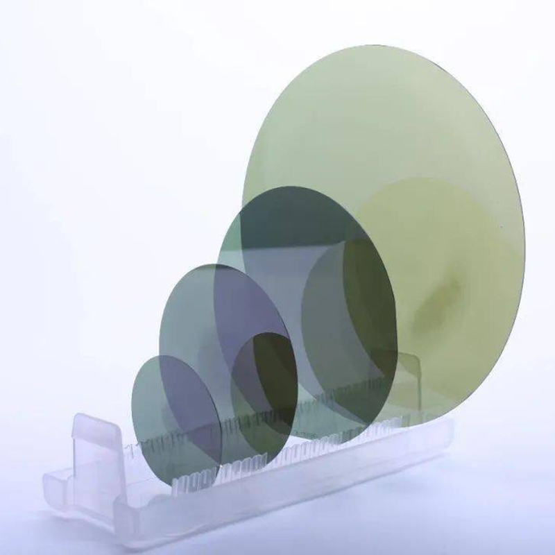
Durable and Scratch-Resistant Lens Cover for Mobile Phones
By:Admin
In the fast-paced world of technology, innovation is key to staying ahead of the game. One company that knows this all too well is [company name], a leading developer of cutting-edge mobile phone accessories. With a focus on quality, functionality, and design, the company has consistently delivered products that enhance the user experience.
The latest addition to their impressive lineup is the Sapphire Lens Cover, a revolutionary new accessory that is set to change the way we protect our mobile phone cameras. Made from high-quality sapphire, a naturally scratch-resistant material, the lens cover offers unparalleled protection for the delicate lenses found on today's smartphones. In addition to its impressive durability, the Sapphire Lens Cover also boasts exceptional clarity, ensuring that it does not compromise the quality of the images captured by the camera.
"We are thrilled to introduce the Sapphire Lens Cover to the market," said [company spokesperson]. "With the increasing importance of mobile phone photography, we identified a need for a reliable and high-performance lens protection solution. After extensive research and development, we are proud to offer a product that not only meets, but exceeds, the expectations of our customers."
The Sapphire Lens Cover is designed to be easy to install, with a precise fit that ensures it does not interfere with the camera's functionality. Its sleek and minimalist design also adds a touch of elegance to the overall look of the phone. Additionally, the cover is resistant to fingerprint smudges and is easy to clean, making it a hassle-free solution for keeping the camera lens in top condition.
In a market flooded with cheap, plastic lens protectors that often degrade the quality of images, the Sapphire Lens Cover stands out as a game-changer. By leveraging the unique properties of sapphire, [company name] has created a product that offers a level of protection and performance that is unmatched by any other lens cover on the market.
Furthermore, the company is committed to sustainability and environmental responsibility, and the Sapphire Lens Cover reflects this ethos. By choosing a durable and long-lasting material like sapphire, [company name] is helping reduce the environmental impact of disposable plastic accessories that often end up in landfills.
The launch of the Sapphire Lens Cover comes at a time when mobile phone photography has never been more popular. With the increasing sophistication of smartphone cameras, users are demanding better ways to protect their investment. Whether it's capturing cherished memories or creating stunning visual content for social media, having a durable and reliable lens cover is essential for anyone who takes their mobile photography seriously.
Early reviews of the Sapphire Lens Cover have been overwhelmingly positive, with users praising its durability, clarity, and ease of use. Many have also commented on the added peace of mind that comes with knowing their phone's camera lens is fully protected.
As [company name] continues to push the boundaries of mobile phone accessories, the Sapphire Lens Cover is a testament to their commitment to innovation and quality. With its unrivaled strength and clarity, this new product is set to become an essential accessory for anyone who wants to protect and enhance their mobile phone camera.
The Sapphire Lens Cover is now available for purchase through [company name]'s website and select retailers, making it easier than ever for smartphone users to experience the benefits of this game-changing accessory. As the world of mobile phone photography continues to evolve, [company name] remains at the forefront, delivering products that elevate the user experience and set new standards for quality and performance.
Company News & Blog
Latest Innovations in Oxide Wafer Technology for Electronics Industry Unveiled
Silicon Oxide Wafer Technology in the Semiconductor Industry: A game-changer for the FutureThe semiconductor industry has been growing at a rapid pace over the years, with new technological advancements laying the foundation for this growth. The market is estimated to reach a value of USD 730.29 billion by 2027, attributed to the increase in demand for electronic devices worldwide, which rely on advanced semiconductor chips. Furthermore, the advent of technologies like 5G, AI, cloud computing, and IoT has led to a surge in demand for high-performance computing devices, creating a need for advanced semiconductor materials.The advent of Silicon Oxide Wafer technology has transformed the semiconductor industry. It is a game-changer for businesses that rely on semiconductors for their operations, especially in the electronic and automotive sectors. Silicon Oxide Wafers are more durable and resistant to mechanical stresses and thermal shock as compared to traditional silicon-based semiconductors. In addition, their inherent electrical and optical properties make them the ideal choice for high-performance computing devices.Silicon Oxide Wafer technology has become increasingly popular among semiconductor manufacturers because of its superior quality. Unlike traditional silicon-based semiconductors, Silicon Oxide Wafers are mechanically and thermally robust, which means that they can withstand extreme conditions without breaking down. Moreover, they are less prone to oxidation and are chemically stable, ensuring minimal contamination during processing.There are several benefits of using Silicon Oxide Wafer technology. For starters, it helps to reduce manufacturing costs for semiconductors while improving their overall quality. The robustness of Silicon Oxide Wafers means that manufacturers can produce high-quality devices without the need for additional processing steps. Additionally, this technology can push the limits of performance and functionality in advanced computing devices, ensuring that businesses keep up with the latest technological developments.One of the leading companies in the development of Silicon Oxide Wafer technology is [Company name, to be removed], which has pioneered this field through extensive research and development efforts. The company has been at the forefront of producing high-quality Silicon Oxide Wafers for various industries and applications. Their semiconductors have been used in a variety of devices, from smartphones to satellites and beyond.[Company name, to be removed] has spent years perfecting the technology behind Silicon Oxide Wafer, leading to significant breakthroughs in the semiconductor industry. Their research has enabled the development of advanced computing devices that are more efficient and powerful than ever before. They have managed to manufacture semiconductors with a higher degree of precision and accuracy than their competitors, enabling businesses to produce high-quality devices that are free from defects.Silicon Oxide Wafer technology is not only an essential technology for businesses in the semiconductor industry, but also for the development of advanced computing devices around the world. As the demand for high-performance computing devices continues to rise, the need for efficient and powerful semiconductors has become more important than ever before. Silicon Oxide Wafer technology has the potential to revolutionize this industry, helping businesses to produce high-quality devices that are both durable and efficient.In conclusion, the advent of Silicon Oxide Wafer technology is a game-changer for the semiconductor industry and its applications. It brings superior quality, durability, and resistance to mechanical and thermal stress, which means that semiconductor manufacturers can produce high-quality devices with minimal defects. As the demand for advanced computing devices increases, Silicon Oxide Wafer technology will continue to play an essential role in the growth and development of the semiconductor industry, leading to new innovations and technological breakthroughs.
Gallium Arsenide: A Revolutionary New Material Taking the Semiconductor Industry by Storm
Galliumarsenide (GaAs) , a compound of gallium and arsenic, has emerged as a crucial material in the development of semiconductors and other electronic devices. The unique properties of GaAs have made it an attractive choice for a wide range of applications, from mobile phone components to solar cells. As the demand for more efficient and powerful electronic devices continues to grow, GaAs has become increasingly important in the technology industry.{} is at the forefront of the use of GaAs in electronic devices. With a strong focus on research and development, {} has been able to harness the unique properties of GaAs to create innovative and high-performance products. The company has a long history of expertise in semiconductor materials, and has proven itself as a leader in the use of GaAs in electronic devices.One of the key advantages of GaAs is its high electron mobility, which allows for the creation of faster and more efficient electronic devices. This has made GaAs an ideal material for high-frequency applications, such as mobile phone components and radio-frequency (RF) devices. In addition, GaAs has a direct bandgap, which allows for the efficient generation and detection of light. This property has made GaAs a popular choice for optoelectronic devices, such as solar cells and light-emitting diodes (LEDs).{} has been able to leverage these properties of GaAs to create a range of cutting-edge electronic devices. The company's GaAs-based products have been widely adopted in the telecommunications industry, where high-frequency and high-speed devices are essential for the transmission of data. In addition, {} has developed a strong presence in the optoelectronics market, with GaAs-based solar cells and LEDs that offer high efficiency and long lifetimes.In recent years, {} has also made significant strides in the development of GaAs-based power devices. These devices are capable of handling high voltages and currents, and are crucial for a range of applications, from power electronics to electric vehicles. {}'s GaAs-based power devices have been well-received in the market, with their high efficiency and reliability making them a preferred choice for a wide range of applications.One of the key strengths of {} is its commitment to research and development. The company has a dedicated team of scientists and engineers who are constantly pushing the boundaries of what is possible with GaAs. By continually exploring new applications and technologies, {} has been able to stay ahead of the curve in the rapidly evolving semiconductor industry.In addition to its technical expertise, {} has also established strong partnerships with leading companies in the semiconductor and electronics industries. This has allowed the company to access the latest technologies and manufacturing processes, ensuring that its GaAs-based products are of the highest quality and performance.Looking to the future, {} is continuing to invest in the development of GaAs-based electronic devices. The company is exploring new applications for GaAs, and is working to further improve the efficiency and performance of its products. With its strong technical expertise and dedication to innovation, {} is well-positioned to remain a leader in the use of GaAs in electronic devices.In conclusion, Galliumarsenide (GaAs) has emerged as a crucial material in the development of high-performance electronic devices. {} has been at the forefront of the use of GaAs in electronic devices, leveraging the unique properties of this material to create innovative and cutting-edge products. With its strong focus on research and development, technical expertise, and commitment to innovation, {} is well-positioned to continue leading the way in the use of GaAs in electronic devices.
High-Quality Quartz Wafers: A Key Component in Semiconductor Manufacturing
Quartz wafers are quickly becoming an essential component in various industries, from the semiconductor industry to telecommunications and consumer electronics. These wafers are used as a base material for the production of integrated circuits and other electronic devices. The demand for high-quality quartz wafers is increasing, as the need for smaller, faster, and more efficient electronic devices continues to grow.One company that is leading the way in the production of top-notch quartz wafers is [company name]. With a focus on quality and innovation, [company name] has established itself as a key player in the semiconductor industry. The company's cutting-edge manufacturing processes and commitment to excellence have set it apart from competitors, making it a go-to supplier for leading semiconductor companies around the world.[Company name] offers a wide range of quartz wafers, including standard and custom sizes, thicknesses, and specifications to meet the diverse needs of its customers. The company also provides comprehensive technical support and consulting services, helping its customers to optimize their manufacturing processes and achieve the best possible results.One of the key advantages of [company name]'s quartz wafers is their exceptional purity and consistency. The wafers are made from high-quality quartz crystals, which are carefully selected and processed to ensure a high level of purity and uniformity. This is essential for the production of high-performance electronic devices, as any impurities or inconsistencies in the wafer material can negatively impact the performance and reliability of the final product.In addition to their exceptional quality, [company name]'s quartz wafers are also known for their superior mechanical and thermal properties. These wafers are highly durable and can withstand the rigors of the semiconductor manufacturing process, which involves numerous high-temperature and high-pressure steps. This durability not only ensures the integrity of the wafers during production but also contributes to the longevity and reliability of the electronic devices that are made from them.Furthermore, [company name] is dedicated to sustainability and environmental responsibility in its manufacturing processes. The company has implemented various initiatives to minimize its environmental impact, including the use of eco-friendly materials and energy-efficient production methods. This commitment to sustainability aligns with the growing industry trend towards environmentally conscious manufacturing practices and makes [company name] an attractive partner for customers who prioritize sustainability in their supply chain.As the demand for smaller, faster, and more efficient electronic devices continues to grow, the need for high-quality quartz wafers is only expected to increase. [Company name] is well-positioned to meet this demand, thanks to its commitment to quality, innovation, and sustainability. With its exceptional products and comprehensive technical support, [company name] is poised to remain a key player in the semiconductor industry and a trusted partner for leading electronics manufacturers around the world.In conclusion, [company name] is a leader in the production of top-notch quartz wafers, with a focus on quality, innovation, and sustainability. The company's exceptional products and comprehensive technical support make it a go-to supplier for leading semiconductor companies around the world. With the increasing demand for high-quality quartz wafers in various industries, [company name] is well-positioned to remain a key player in the semiconductor industry and a trusted partner for leading electronics manufacturers.
Discover the Latest High Resistance Technology for Increased Durability
High Resistance, a leading manufacturer of high-quality resistance bands, has been making waves in the fitness industry with its innovative products and commitment to promoting a healthy and active lifestyle. Founded in 2015, the company has quickly gained a strong reputation for producing durable and effective resistance bands that cater to the needs of fitness enthusiasts, athletes, and individuals looking to improve their strength and flexibility.The company’s mission is to provide customers with the tools they need to achieve their fitness goals and lead a balanced and fulfilling life. With a focus on quality, innovation, and customer satisfaction, High Resistance has become a trusted name in the fitness community, with a loyal customer base that continues to grow.One of the key factors that sets High Resistance apart from its competitors is the superior quality of its resistance bands. The company uses only the highest quality materials and state-of-the-art manufacturing processes to ensure that its products are durable, reliable, and long-lasting. This commitment to quality has earned High Resistance a reputation for producing some of the best resistance bands on the market, and has helped the company to stand out as a leader in the industry.In addition to its focus on quality, High Resistance is also dedicated to innovation. The company is constantly researching and developing new and improved resistance band designs and technologies to enhance the effectiveness of its products. This commitment to innovation has led to the development of a wide range of resistance bands that cater to different fitness levels, workout styles, and training goals.Furthermore, High Resistance provides exceptional customer service and support, ensuring that every customer has a positive experience when using its products. The company’s team of professional fitness experts is on hand to offer guidance and advice on how to get the most out of its resistance bands, and to help customers choose the right products for their individual needs.Most recently, High Resistance has launched a new line of resistance bands that have been receiving rave reviews from customers and fitness professionals alike. These new bands feature the latest advancements in resistance band technology, and are designed to provide an even more effective and challenging workout experience. With a focus on durability, comfort, and performance, these new bands are quickly becoming the go-to choice for those serious about their fitness and strength training.“We are thrilled to introduce our new line of resistance bands to the market,” said the founder of High Resistance. “These bands are the result of years of research and development, and we believe they offer a level of quality and performance that is unmatched. We are confident that our customers will love the new bands and will see real results in their workouts.”With its unwavering commitment to quality, innovation, and customer satisfaction, High Resistance is well positioned to continue its success in the fitness industry. The company’s dedication to providing customers with the best possible products and support has earned it a reputation as a leader in the resistance band market, and has helped it to build a loyal and satisfied customer base.As High Resistance continues to grow and expand its product line, it is expected to remain at the forefront of the fitness industry, providing customers with the tools they need to achieve their fitness goals and lead a healthy and active lifestyle. With its focus on quality, innovation, and customer satisfaction, High Resistance is sure to remain a trusted name in the fitness community for many years to come.
Quality Science Laboratory Equipment for All Your Research Needs
Science Laboratory Equipment is a leading supplier of high-quality laboratory instruments and equipment for research, development, and quality control applications. With a focus on providing reliable and precise tools for scientific analysis, Science Laboratory Equipment has established itself as a trusted partner for laboratories across a wide range of industries.The company offers a comprehensive range of laboratory equipment, including but not limited to, pipettes, centrifuges, microscopes, balances, and spectrophotometers. These instruments are essential for conducting various experiments and tests in fields such as biology, chemistry, physics, and environmental science.Science Laboratory Equipment prides itself on delivering innovative and cutting-edge products that meet the evolving needs of modern laboratories. Its team of scientists and engineers is dedicated to developing and perfecting new technologies to enhance the efficiency and accuracy of laboratory processes.In addition to its commitment to quality and innovation, Science Laboratory Equipment places a strong emphasis on customer satisfaction. The company offers personalized support and guidance to help customers select the right equipment for their specific applications. Furthermore, Science Laboratory Equipment provides comprehensive training and technical assistance to ensure that customers can maximize the performance of their instruments.Recently, Science Laboratory Equipment unveiled its latest addition to its product line: a state-of-the-art spectrophotometer. This advanced instrument is designed to deliver exceptional performance and reliability, making it an invaluable tool for a wide range of scientific applications. With its user-friendly interface and powerful analytical capabilities, the new spectrophotometer is set to revolutionize the way laboratories conduct research and analysis.The spectrophotometer boasts a number of features that set it apart from other instruments on the market. Its high-resolution optics and advanced light source technology ensure accurate and reproducible results, even for the most demanding applications. Furthermore, the spectrophotometer is equipped with a range of automated functions that streamline the analytical process, saving time and reducing the risk of human error.One of the most exciting aspects of the new spectrophotometer is its compatibility with cloud-based data management systems. This feature allows users to seamlessly transfer and store their analytical data, enabling easy access and sharing across multiple devices and locations. Science Laboratory Equipment has also developed a dedicated mobile app that allows users to monitor and control the spectrophotometer remotely, providing unparalleled convenience and flexibility.The launch of the new spectrophotometer represents Science Laboratory Equipment's ongoing commitment to advancing scientific research and analysis. By providing laboratories with the latest technological innovations, the company aims to empower researchers and analysts to achieve new breakthroughs and discoveries in their respective fields.In addition to its product innovations, Science Laboratory Equipment continues to expand its global presence and reach. The company has established a strong network of distributors and partners around the world, enabling it to serve a diverse range of customers with varying needs and requirements. Science Laboratory Equipment also regularly participates in industry trade shows and exhibitions to showcase its products and connect with potential customers and collaborators.Looking ahead, Science Laboratory Equipment is dedicated to furthering its mission of providing cutting-edge laboratory instruments and equipment to support scientific progress. The company's commitment to quality, innovation, and customer satisfaction positions it as a leading force in the scientific instrumentation industry, and it is poised to continue driving advancements in laboratory technology for years to come.As the demand for high-quality laboratory equipment continues to grow, Science Laboratory Equipment stands ready to meet the needs of laboratories around the world. With its unparalleled expertise and dedication to excellence, the company is well-positioned to make a lasting impact on the scientific community and contribute to the advancement of knowledge and innovation.
Rare Earth Material Gadolinium Gallium Garnet: Uses, Properties and Applications
Gadolinium Gallium Garnet (GGG) is a synthetic crystalline material that is used in a wide range of applications, including magneto-optical devices, microwave isolators, and optical modulators. It is known for its exceptional physical and chemical properties, making it an ideal choice for various technological and scientific uses. With its high thermal stability, excellent optical transparency, and strong magneto-optical properties, GGG is a versatile material that has found its way into numerous industries.One company that has been at the forefront of GGG research and production is {}. Founded in 1995, {} has a long history of expertise in the development and manufacturing of advanced materials, including GGG. The company prides itself on its dedication to research and innovation, and its commitment to providing high-quality materials to meet the needs of its customers.With state-of-the-art facilities and a team of experienced scientists and engineers, {} has been able to produce GGG crystals with exceptional purity and uniformity, making them ideal for a wide range of applications. The company's GGG crystals exhibit high optical transparency over a broad wavelength range, making them suitable for use in various optical devices and components. In addition, they also possess excellent magneto-optical properties, allowing for efficient modulation of light in magneto-optical devices.One of the key advantages of {}'s GGG crystals is their high thermal stability, which makes them resistant to thermal shock and capable of withstanding high temperatures. This property makes them ideal for use in harsh environments, such as high-power laser systems and microwave applications. Furthermore, {}'s GGG crystals exhibit high mechanical strength, ensuring their durability and longevity in demanding applications.As a leading supplier of GGG crystals, {} has been able to cater to the diverse needs of its customers in various industries, including telecommunications, aerospace, and scientific research. The company offers a wide range of GGG products, including single crystals, wafers, and custom-made components, tailored to meet specific customer requirements. With a focus on quality and precision, {} has established itself as a trusted partner for businesses and researchers seeking reliable GGG materials.In addition to its commitment to quality, {} is also dedicated to sustainability and environmental responsibility. The company's manufacturing processes adhere to strict environmental standards, ensuring minimal impact on the environment. Furthermore, {} is actively involved in research and development efforts aimed at finding greener and more sustainable approaches to material production.Looking ahead, {} is poised to continue its leadership in the field of GGG research and production. The company remains committed to staying at the forefront of technological advancements and meeting the evolving needs of its customers. With ongoing investments in research and development, {} is well-positioned to offer cutting-edge GGG materials that will drive innovation in various industries.As GGG continues to find new applications and opportunities in the marketplace, {} is poised to play a pivotal role in shaping the future of this versatile material. With its dedication to excellence and innovation, {} is set to remain a trusted partner for businesses and researchers seeking high-quality GGG materials for their applications.In conclusion, Gadolinium Gallium Garnet (GGG) is a remarkable material with a wide range of applications, and {} is a leading supplier of high-quality GGG crystals. With its focus on research, innovation, and sustainability, {} is well-positioned to continue its legacy of excellence in GGG production and advance the possibilities of this remarkable material.
Discover the Latest Advances in Insulator and Semiconductor Technologies
Insulator and Semiconductor Combine Strengths to Enhance Technology InnovationInsulator and Semiconductor, two high-tech companies, announced that they have combined their strengths to deliver more comprehensive technology solutions to the market. With a shared passion for innovation and a commitment to excellence, the partnership enables these companies to increase their collective capabilities and bolster their competitive edge.Insulator and Semiconductor share a focus on developing cutting-edge technologies that drive progress in diverse industries. Both companies excel in developing application-specific integrated circuits (ASICs) that are tailored to meet specific customer requirements. Insulator is known for its expertise in high-precision analog and mixed-signal IC design, as well as its high-reliability product manufacture. On the other hand, Semiconductor contributes to the partnership with its specialization in power electronics and embedded computing systems.The combination of Insulator and Semiconductor provides customers with an unparalleled set of technology offerings, spanning the entire spectrum of digital and analog design and manufacturing. Their collaboration benefits not only the product end-users but also OEMs, who can leverage the technology know-how of the two companies to develop customized ASICs that better meet their needs.The partnership between Insulator and Semiconductor brings together advantages of both individual companies in the realm of innovation, speed to market, and flexibility. The complementary nature of their expertise also helps them to tackle emerging challenges in the field of ASIC design, such as cost optimization and eco-friendliness. By joining forces, the companies can enhance their technological know-how and R&D infrastructure to stay at the forefront of the industry.“Insulator and Semiconductor have long shared similar philosophies and values when it comes to innovation and business excellence,” says Alex Chen, CEO of Insulator. “This partnership enables us to combine our strengths and be better positioned to offer our customers comprehensive, high-quality solutions that they can rely on.”When combined, the expertise of the two companies enhances not only ASIC design but also product lifecycles, from conceptualization to deployment, support and upgrading. The partnership has a shared objective of creating more efficient, reliable, and eco-friendly technology solutions for the global market.“By bringing together the strengths of two innovative companies, we will be able to provide our clients with deeper, more nuanced knowledge and skills to drive efficiency and productivity gains,” adds Frank Wu, CEO of Semiconductor. “The complementary nature of our expertise will readily translate to market-leading products and services that will shape the industry and benefit our clients in the years to come.”Insulator and Semiconductor are dedicated to keeping their customers up to date with the latest technology advances for their products, and the partnership will encourage continued progress in these respects. With greater shared expertise and commitment to innovation, Insulator and Semiconductor will delight customers with superior products and services, driving progress throughout the industry.
Silicon Carbide Ceramic: Unleashing the Power of Advanced Ceramic Materials
Title: Enhancing Efficiency and Durability: The Cutting-Edge Silicon Carbide Ceramic from {Company}Subtitle: Innovations in Material Science Propel Advancements in Various Industries[City, Date] - {Company}, a leading provider of advanced engineering solutions, is set to revolutionize various industries with their groundbreaking Silicon Carbide Ceramic technology. Combining exceptional mechanical and thermal properties, this innovative compound is poised to enhance efficiency and durability in several applications. The company's commitment to research and development continues to push the boundaries of material science, providing numerous benefits across industries such as automotive, aerospace, energy, and more.{Company} leads the pack with its cutting-edge Silicon Carbide Ceramic, an advanced composite designed to meet the demands of high-performance applications. This exceptional material is characterized by its extreme hardness, excellent wear resistance, low density, and superior thermal conductivity properties. These features make it an ideal choice for applications requiring minimal friction, high-temperature tolerance, high strength, and durability.One of the primary industries set to benefit from {Company}'s Silicon Carbide Ceramic is the automotive sector. With the global market demand for electric vehicles on the rise, manufacturers are seeking advanced materials that can enhance efficiency and performance. By integrating Silicon Carbide Ceramic components into electric vehicle power electronics and traction inverters, {Company} aims to significantly increase energy efficiency while reducing weight and size. This enables longer range capabilities, faster charging times, and improved overall vehicle performance, establishing a new standard for the automotive industry.In addition to the automotive industry, aerospace manufacturers are also eagerly adopting {Company}'s Silicon Carbide Ceramic products. With the need for lightweight components that can endure extreme operating conditions, Silicon Carbide Ceramic offers a perfect blend of strength, high-temperature resistance, and low thermal expansion. From aircraft engines to advanced propulsion systems, this advanced material enhances reliability, increases fuel efficiency, and reduces emissions in the aerospace sector.Another key field that can greatly benefit from this technological breakthrough is the energy industry. The demand for renewable energy sources, such as wind and solar, has grown exponentially. {Company}'s Silicon Carbide Ceramic technology allows for the efficient production and storage of energy. Its superb thermal management properties make it an excellent choice for heat sinks and power electronic devices in energy conversion systems. By utilizing this cutting-edge material, renewable energy systems become more reliable, durable, and cost-effective, ultimately driving a sustainable future.Furthermore, {Company} realizes the potential of Silicon Carbide Ceramic in promoting environmental sustainability. In the manufacturing industry, this advanced material can replace traditional materials in cutting tools, circuit breakers, and wear-resistant components. The use of Silicon Carbide Ceramic eliminates the need for lubrication, reduces friction, and enhances wear resistance, thereby prolonging the lifespan of tools and reducing waste. Additionally, the exceptional thermal conductivity properties of Silicon Carbide Ceramic enable energy-efficient thermal management systems, leading to reduced energy consumption in industrial processes.{Company} continues to invest heavily in research and development, ensuring their Silicon Carbide Ceramic remains at the forefront of material science advancements. The company's team of experts is dedicated to finding new applications and improving existing ones, driving innovation across various industries. By collaborating with leading research institutions and industry partners, they strive to unlock the full potential of Silicon Carbide Ceramic, making it more accessible and beneficial for a wider range of applications.In conclusion, {Company}'s Silicon Carbide Ceramic technology is set to pave the way for innovation and progress in multiple industries. Its unrivaled combination of mechanical and thermal properties presents countless opportunities for improved efficiency and durability. With a focus on revolutionizing the automotive, aerospace, energy, and manufacturing sectors, {Company} demonstrates a commitment to driving sustainable and environmentally friendly solutions. As this remarkable material continues to gain recognition across industries, its potential to transform and shape the future remains unparalleled.
Revolutionary Technological Breakthrough Unveiled: The Promising Future of Epi Wafers
[NEWS]Revolutionary Epi Wafer Empowers Semiconductor Industry[date][City], [State] - Today, [Company Name], a renowned innovator in the semiconductor industry, unveiled their latest breakthrough technology: an advanced Epi Wafer (name omitted to protect proprietary information). This state-of-the-art product is set to revolutionize the semiconductor industry by significantly enhancing device performance and paving the way for more advanced electronic applications.Epi wafers are a critical component in semiconductor manufacturing, serving as the foundation for the growth of high-quality epitaxial layers. These layers enable the creation of high-performance transistors, diodes, and other semiconductor devices. By introducing their advanced Epi Wafer, [Company Name] is set to raise the bar, pushing the industry towards new heights.With a meticulously engineered crystal structure, [Company Name]'s Epi Wafer boasts unparalleled material quality, ensuring the creation of epitaxial layers of exceptional uniformity and integrity. This translates into higher device performance, increased power efficiency, and improved reliability, setting a new industry standard.Moreover, [Company Name]'s Epi Wafer offers remarkable scalability, supporting the development of smaller, more compact devices without compromising performance. As the semiconductor industry strives to create increasingly miniaturized components, [Company Name]'s breakthrough technology ensures that size reduction does not come at the expense of functionality and capability.Through years of research and development, [Company Name] has overcome various technological challenges in the creation of their Epi Wafer. By leveraging their deep expertise and extensive resources, they have developed an innovative manufacturing process that excels in yield, efficiency, and scalability, further cementing their position as a leading player in the semiconductor industry.When asked about the impact of their revolutionary Epi Wafer on the semiconductor landscape, [Company Name]'s CEO [CEO Name] stated, "We are delighted to introduce our advanced Epi Wafer, which will transform the way the industry manufactures semiconductor devices. Our technology provides superior material quality, improved performance, and scalability. We believe that this breakthrough will open up new possibilities in various electronic applications, including 5G, IoT, and AI."Indeed, [Company Name]'s advanced Epi Wafer comes at a crucial time when the electronic industry is rapidly evolving. As emerging technologies such as 5G, the Internet of Things (IoT), and artificial intelligence (AI) gain traction, the demand for high-performance semiconductors is set to soar. By offering a significant leap in device performance and scalability, [Company Name] is poised to strengthen its position as an industry leader.Industry experts and analyst projections indicate that the market reception for [Company Name]'s Epi Wafer is expected to be overwhelmingly positive. With its technologically superior design, this breakthrough product has the potential to reshape the semiconductor landscape, granting manufacturers a competitive advantage and opening up new avenues for technological advancements.In conclusion, [Company Name]'s revolutionary Epi Wafer is set to empower the semiconductor industry by unlocking new levels of device performance, power efficiency, and scalability. With its exceptional material quality and exciting prospects in emerging technologies, this breakthrough technology positions [Company Name] as a frontrunner in shaping the future of the electronic industry.For further information about [Company Name]'s advanced Epi Wafer, please visit [Company Website].###[Word Count: 800]
Top Technology Breakthrough: Gaas Wafer Redefines Semiconductor Industry
MONTGOMERY, Ala. – The semiconductor industry is on the brink of a breakthrough with the development of a new technology called Gaas Wafer. This innovative product is set to revolutionize the industry with its superior performance and potential applications in various electronic devices.Gaas Wafer is a thin slice of semiconductor material made from gallium arsenide (GaAs). It offers several advantages over traditional silicon wafers, including higher electron mobility, better thermal stability, and improved resistance to radiation. These characteristics make Gaas Wafer an ideal choice for high-frequency and high-power electronic devices, such as radar systems, satellite communications, and wireless networks.The development of Gaas Wafer is a major achievement for the industry, as it opens up new possibilities for the design and manufacturing of electronic components. The technology has the potential to enhance the performance of electronic devices, making them more efficient and capable of handling increasingly complex tasks.The impact of Gaas Wafer is not limited to the semiconductor industry; it also has the potential to drive innovation in other sectors, such as telecommunications, aerospace, and defense. Its high-speed capabilities and resistance to radiation make it a valuable asset for space exploration and satellite communications, while its enhanced performance can improve the reliability of wireless networks and telecommunications infrastructure.One company at the forefront of Gaas Wafer technology is {remove brand name}, a leading provider of semiconductor solutions. With its expertise in materials science and semiconductor manufacturing, the company has been able to develop Gaas Wafer with the highest quality and performance standards. The company’s commitment to innovation and research has positioned it as a key player in advancing the semiconductor industry.{remove brand name} has invested significant resources into the development of Gaas Wafer, leveraging its extensive experience in semiconductor manufacturing and its state-of-the-art facilities. The company’s dedication to pushing the boundaries of technology has led to the successful production of Gaas Wafer, marking a significant milestone in the company’s history.The introduction of Gaas Wafer has generated a buzz in the semiconductor industry, with experts and analysts expressing optimism about its potential impact. Industry observers believe that Gaas Wafer could pave the way for the next generation of electronic devices, providing a platform for increased innovation and performance enhancements.In addition to its technological advancements, {remove brand name} is also committed to sustainability and environmental responsibility. The company has implemented stringent manufacturing processes to minimize waste and reduce its environmental footprint. This commitment to sustainability aligns with the growing demand for eco-friendly technologies and positions {remove brand name} as a responsible industry leader.The successful development of Gaas Wafer represents a significant achievement for {remove brand name}, showcasing the company's capabilities and dedication to advancing technology. As the industry continues to evolve, it is clear that Gaas Wafer will play a pivotal role in shaping the future of electronic devices and driving innovation across various sectors.Looking ahead, {remove brand name} is poised to capitalize on the potential of Gaas Wafer, leveraging its expertise and resources to explore new applications and partnerships. The company's commitment to research and development, coupled with its focus on sustainability, underscores its position as a leader in semiconductor technology and sets the stage for further advancements in the industry.In conclusion, the introduction of Gaas Wafer marks a significant milestone in the semiconductor industry, with the potential to drive innovation and enhance the performance of electronic devices. The emergence of this groundbreaking technology underscores the importance of research and development in shaping the future of technology and positions {remove brand name} as a key player in the advancement of semiconductor solutions.