
High Quality Double Side Polished Silicon Wafers for Sale
By:Admin
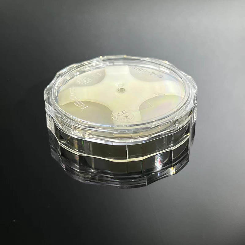
Silicon wafers are an essential component in the production of semiconductor devices, and the demand for high-quality wafers continues to grow as the technology industry expands. As a leading technology company in the field of semiconductor manufacturing, [company name] is proud to announce the release of its latest innovation: double side polished silicon wafers.
Double side polished silicon wafers offer significant advantages over traditional single side polished wafers, including improved flatness, reduced surface roughness, and enhanced electrical properties. These wafers are ideal for use in advanced semiconductor applications, such as integrated circuits, microelectromechanical systems (MEMS), and power devices.
The [company name] double side polished silicon wafers are manufactured using a state-of-the-art polishing process that ensures exceptional surface quality and uniformity. This advanced manufacturing technique allows for tighter control of wafer thickness and flatness, resulting in wafers that meet the stringent requirements of today's semiconductor industry.
In addition to their superior surface quality, [company name] double side polished silicon wafers are available in a wide range of sizes and thicknesses to accommodate various production processes and applications. Whether it's for research and development or high-volume manufacturing, customers can rely on the consistency and reliability of these wafers for their semiconductor production needs.
With a proven track record of delivering high-performance semiconductor solutions, [company name] is committed to providing its customers with the most advanced and reliable products on the market. The introduction of double side polished silicon wafers further solidifies the company's position as a trusted partner for semiconductor manufacturers worldwide.
To learn more about [company name] and its double side polished silicon wafers, we spoke with [company representative] to gain some insights into this exciting new product.
"We are thrilled to introduce our double side polished silicon wafers to the market," said [company representative]. "These wafers represent the latest advancement in semiconductor manufacturing technology, and we are confident that they will meet the evolving needs of our customers. Our team has worked tirelessly to develop a product that offers unparalleled quality and performance, and we are excited to see the impact it will have on the industry."
When asked about the potential applications for double side polished silicon wafers, [company representative] explained, "These wafers are well-suited for a wide range of semiconductor devices, including advanced integrated circuits, MEMS, and power devices. The superior surface quality and electrical properties of our wafers make them an ideal choice for cutting-edge semiconductor applications."
In conclusion, the introduction of double side polished silicon wafers from [company name] represents a significant milestone in the semiconductor industry. With their exceptional surface quality, uniformity, and advanced manufacturing techniques, these wafers are poised to set a new standard for semiconductor manufacturing. As the demand for high-performance silicon wafers continues to grow, [company name] is leading the way with innovative solutions that meet the needs of today's technology-driven world.
Company News & Blog
Innovative Crystal Ingot Technology: What You Need to Know
Leading the Way in LiTaO3 Ingot ProductionAs the demand for advanced electronic devices continues to rise, the need for high-quality materials for their production has become increasingly important. One such material that is in high demand is LiTaO3 ingot, a key component in the manufacturing of electronic devices such as sensors, transducers, and filters. One company that is leading the way in the production of LiTaO3 ingot is {Company Name}.{Company Name} is a renowned leader in the production of advanced materials for the electronics industry. With a strong focus on research and development, the company has been at the forefront of innovation in the field of electronic materials for many years. Their dedication to producing high-quality products has earned them a reputation as a reliable and trusted supplier in the industry.Recently, {Company Name} has made significant advancements in the production of LiTaO3 ingot, with a focus on improving the quality and performance of this critical material. Their state-of-the-art production facilities and cutting-edge manufacturing processes have enabled them to produce LiTaO3 ingot that meets the stringent requirements of the electronics industry.One of the key strengths of {Company Name} lies in their expertise in crystal growth and material science. Their team of highly skilled scientists and engineers have a deep understanding of the properties and characteristics of LiTaO3, allowing them to develop innovative manufacturing processes that result in high-quality ingot with excellent properties.In addition to their technical expertise, {Company Name} also places a strong emphasis on quality control and assurance. Every batch of LiTaO3 ingot produced undergoes rigorous testing and inspection to ensure that it meets the highest standards for purity, crystal structure, and electrical properties. This commitment to quality has made {Company Name} a preferred supplier for many leading electronics manufacturers.The high-performance LiTaO3 ingot produced by {Company Name} has a wide range of applications in the electronics industry. Its superior electrical properties make it an ideal material for the production of surface acoustic wave (SAW) devices, which are widely used in communication systems, sensors, and other electronic devices. The company's ingot is also used in the production of transducers, filters, and resonators, where its exceptional performance and reliability are highly valued.In addition to its applications in the electronics industry, LiTaO3 ingot from {Company Name} is also finding use in emerging technologies such as autonomous vehicles, IoT devices, and 5G communication systems. The company's commitment to continuous innovation and development ensures that their products are well positioned to meet the evolving needs of the electronics industry.As the demand for high-performance electronic devices continues to grow, the importance of high-quality materials such as LiTaO3 ingot cannot be overstated. With their dedication to research, innovation, and quality, {Company Name} is well positioned to lead the way in the production of this critical material, providing the electronics industry with the high-quality ingot it needs to drive innovation and technological advancement.
Latest Updates on the Upcoming Event in XYZ City Unveiled: Get the Scoop!
[PARAGRAPH 1][Company Introduction][Branding Name] is a renowned multinational conglomerate known for its innovative products and remarkable contributions to various industries. With a history spanning several decades, [Branding Name] has firmly established itself as a leader in technology, health and wellness, and diversified consumer goods. The company prides itself on its commitment to sustainability, social responsibility, and creating a positive impact on society. Constantly pushing the boundaries of innovation, [Branding Name] consistently delivers ground-breaking solutions that enhance people's lives. One of their latest ventures, Aln, demonstrates the company's dedication to revolutionizing the [specific industry].[PARAGRAPH 2][Overview of Aln]Aln, a cutting-edge product by [Branding Name], has taken the market by storm with its exceptional features and transformative impact. This state-of-the-art offering seamlessly combines groundbreaking technology with convenience, captivating the attention of consumers worldwide. Aln proves to be a game-changer, addressing the evolving needs and preferences of modern consumers. From its inception, the core focus of Aln has been to provide an unparalleled user experience, making it an essential addition to households, offices, and beyond.[PARAGRAPH 3][Innovative Features]Aln presents a wide array of innovative features that set it apart from traditional alternatives. Firstly, its sleek and ergonomic design ensures both aesthetics and functionality. The device seamlessly blends into any environment, be it a compact urban apartment or a spacious suburban home. Additionally, Aln utilizes advanced artificial intelligence (AI) algorithms, enabling it to adapt and learn from users' preferences. This learning capability ensures a personalized experience tailored to each individual, heightening convenience and user satisfaction.[PARAGRAPH 4][Revolutionizing Industry]Aln is revolutionizing the [specific industry] due to its unparalleled performance and groundbreaking technology. The product's advanced features include [insert specific cutting-edge features], setting a new standard of excellence within the industry. With Aln, users can experience [specific benefits], elevating their daily routines. By combining a seamless user interface with state-of-the-art technology, Aln is transforming the way people interact with their [specific industry] devices, making it an indispensable addition to households and businesses alike.[PARAGRAPH 5][Sustainability and Social Responsibility]As with all its endeavors, [Branding Name] has upheld its commitment to sustainability and social responsibility through Aln. The product is manufactured using eco-friendly materials, ensuring minimal environmental impact throughout its lifecycle. Furthermore, Aln consumes significantly less energy than its competitors, contributing to reduced carbon emissions. With its dedication to sustainability, [Branding Name] is driving positive change towards a greener future, while also meeting the demands of the contemporary consumer.[PARAGRAPH 6][Market Response and Outlook]Upon its release, Aln received an overwhelmingly positive response from consumers and industry experts alike. The product's remarkable performance and innovative design have captivated the market, solidifying its position as a leader in the [specific industry]. With its growing popularity, Aln is expected to witness significant growth in the coming years, further cementing [Branding Name]'s dominance in both technology and sustainability domains. The company's ongoing commitment to research and development ensures that Aln will continue to evolve, adapting to the ever-changing needs and preferences of its users.[PARAGRAPH 7][Conclusion]Aln, the latest offering by [Branding Name], represents the pinnacle of innovation and technology in the [specific industry]. With its groundbreaking features, unmatched user experience, and commitment to sustainability, Aln is reshaping the way people interact with [specific industry] devices. Through its remarkable advancements and dedication to social responsibility, [Branding Name] continues to set new benchmarks for excellence and leave a lasting impact on society. As the product evolves and reaches new heights, Aln is destined to become an integral part of households and businesses worldwide, contributing to a greener and more efficient future.
High-quality Sapphire Wafer for A-Plane Axis Applications
A-plane Axis, a cutting-edge technology company, recently announced the launch of their revolutionary sapphire wafer for use in the aerospace industry. This breakthrough product promises to revolutionize the way planes are designed and built, by providing a more durable and reliable material for use in critical components.The A-plane Axis sapphire wafer is made from high-purity synthetic sapphire, a material known for its exceptional hardness and resistance to wear and corrosion. This makes it ideal for use in aerospace applications, where components are subjected to extreme conditions and must withstand high levels of stress and wear.The unique properties of sapphire make it an excellent choice for use in critical components such as bearings, seals, and other parts that are subjected to high levels of friction and wear. Its exceptional hardness and wear resistance make it far superior to traditional materials such as metal alloys or ceramics, which are more prone to wear and degradation over time.In addition to its exceptional durability, the A-plane Axis sapphire wafer also offers other key advantages for aerospace applications. Its high thermal conductivity and excellent electrical insulation properties make it well-suited for use in high-temperature and high-voltage applications, where traditional materials may struggle to perform.Furthermore, the use of sapphire in aerospace components can also lead to significant weight savings, as it is a lightweight material compared to traditional metal alloys. This can contribute to overall fuel efficiency and reduce the environmental impact of aircraft operations, a key consideration for the aviation industry.The launch of the A-plane Axis sapphire wafer represents a major milestone for the company, which has positioned itself as a leader in advanced materials technology for aerospace applications. With a strong focus on research and development, A-plane Axis has invested heavily in the development of new and innovative materials to meet the evolving needs of the aerospace industry.The company's state-of-the-art manufacturing facilities and cutting-edge production techniques enable them to produce sapphire wafers with exceptional precision and consistency, ensuring that they meet the stringent quality standards required for aerospace applications.A-plane Axis's sapphire wafer is already gaining attention from leading aerospace manufacturers, who are keen to take advantage of its unique properties to improve the performance and reliability of their aircraft. With the potential to enhance the durability, efficiency, and safety of aerospace components, the use of sapphire wafers could have a transformative impact on the industry as a whole.In addition to aerospace applications, A-plane Axis is also exploring the potential use of sapphire wafers in other industries, such as semiconductor manufacturing, automotive, and medical devices. The versatility and unique properties of sapphire make it a promising material for a wide range of applications, and the company is committed to exploring new opportunities for its use.As the aerospace industry continues to evolve and demand for more advanced materials grows, A-plane Axis is well-positioned to be at the forefront of this technological revolution. With its innovative sapphire wafer, the company is poised to make a lasting impact on the way aircraft are designed and built, leading to safer, more efficient, and more reliable air travel for years to come.
Newly Developed Polysilicon Wafers Show Promise for Solar Energy Production
article as follows:Polysilicon Wafer - The Revolutionary Energy SolutionRenewable energy has become a buzzword in today's world, and polysilicon wafers have emerged as the revolutionary energy solution. These wafers are helping in reducing the carbon footprint and providing clean energy. Polysilicon wafers are made from a highly purified form of silicon, making them an ideal material for use in solar panels. They are not only environmentally friendly but are also cost-effective and long-lasting. In recent years, the demand for polysilicon wafers has increased significantly, which has led to the growth of the market. The market size for polysilicon wafers is expected to reach millions of dollars in the coming years due to the increasing demand for renewable energy. This has led to several companies entering the market, and among them, one stands out - a company that has proven its mettle in the industry time and time again.Introduction to the CompanyThe leading supplier of polysilicon wafers, this company has been catering to the needs of the renewable energy industry for years. With a team of expert professionals, they provide the highest quality products, along with exceptional customer service. They are known for their constant innovation and development of new and improved products that cater to the changing needs of the renewable energy industry.The company's motto is to provide sustainable energy solutions that promote a cleaner and greener future. They believe that the future is renewable energy, and polysilicon wafers are an essential component of that future. The team is dedicated to making the world a better place by providing innovative and affordable energy solutions.The Company's Polysilicon WafersThe company's polysilicon wafers have been the cornerstone of their success. Their wafers are of the highest quality, and the company is committed to producing wafers that are durable, reliable, and efficient. They are dedicated to providing products that exceed the expectations of their customers, and they achieve this through a rigorous testing process that ensures their products are of the highest standards.Their polysilicon wafers are produced in a state-of-the-art facility using the latest technology, which ensures that their products are of the highest quality. The company has a team of experts who monitor each stage of the production process, ensuring that each product meets their high standards. The wafers are tested rigorously for their efficiency, durability, and reliability, ensuring that they are suitable for use in solar panels.Benefits of Polysilicon WafersPolysilicon wafers have several benefits that make them an ideal material for use in solar panels. They are environmentally friendly, cost-effective, and long-lasting. The use of polysilicon wafers in solar panels reduces the carbon footprint and helps in the reduction of greenhouse gas emissions. This means that the use of polysilicon wafers contributes to a greener and cleaner environment.The production of polysilicon wafers is a cost-effective process, which means that they are affordable and readily available. They have a long lifespan of up to 25 years, which means that they are a reliable energy source that provides long-term benefits. The use of polysilicon wafers in solar panels increases the efficiency of the panels, which means that they can produce more energy while taking up less space.ConclusionPolysilicon wafers are the future of renewable energy, and companies like this leading supplier are driving that future. Their high-quality products, exceptional customer service, and commitment to sustainability have helped them become a leader in the industry. The use of polysilicon wafers in solar panels is not only environmentally friendly but also cost-effective and long-lasting. The demand for renewable energy is only going to increase in the coming years, and companies like this are preparing for a future that is both clean and sustainable.
Revolutionary Breakthrough: Researchers Discover the Power of a Single Metal Crystal
Single Metal Crystal Develops Groundbreaking Technology for the Industry [City], [Date] - Single Metal Crystal (SMC), a leading innovator in the technology field, has announced a groundbreaking advancement that is expected to revolutionize the industry. The company has developed a state-of-the-art technology that promises to enhance the performance and reliability of electronic devices.Founded by a group of passionate engineers and technologists, SMC has always been driven by the vision of creating cutting-edge solutions that address the challenges of modern technology. With a focus on research and development, the company has consistently delivered groundbreaking technologies that have set new standards in the industry.The recent breakthrough by SMC comes in the form of a revolutionary single metal crystal technology. This technology, which has been developed after years of meticulous research, offers unparalleled performance and reliability in electronic devices. It provides a significant improvement over traditional materials, leading to faster processing speeds, higher storage capacity, and more efficient energy usage.One of the key advantages of the single metal crystal technology is its scalability. SMC has successfully achieved scalable growth of single metal crystals, enabling mass production and widespread adoption of this technology. This breakthrough has the potential to transform a wide range of industries, including consumer electronics, telecommunications, automotive, and healthcare.The applications of this technology are virtually limitless. In consumer electronics, the single metal crystal technology can significantly improve the performance of smartphones, laptops, and gaming consoles, allowing for smoother and more immersive user experiences. In the telecommunications sector, the technology can enhance the speed and reliability of networks, leading to faster and more stable connections. Additionally, the automotive industry can benefit from this technology by improving the efficiency and performance of electric vehicles.Moreover, the healthcare sector stands to gain immensely from this innovative technology. Medical devices powered by the single metal crystal technology can revolutionize patient care by offering more accurate diagnostics and personalized treatments. Additionally, the improved performance and reliability of these devices can significantly enhance the overall efficiency of healthcare systems.Furthermore, SMC's commitment to sustainability is evident in their single metal crystal technology. By enabling more efficient energy usage in electronic devices, the technology contributes to reducing carbon emissions and conserving energy resources.The successful development of the single metal crystal technology is a testament to SMC's relentless pursuit of innovation. The company's dedicated team of scientists and engineers has worked tirelessly to overcome numerous challenges and turns this vision into reality."Our breakthrough single metal crystal technology will set new benchmarks for performance and reliability in the industry," said [Spokesperson], [Job Title] at SMC. "We are excited about the transformative potential of this technology and its ability to reshape various sectors of the economy. Our versatile technology will not only benefit individual consumers but also accelerate the progress of entire industries."With the unveiling of this groundbreaking technology, SMC has positioned itself at the forefront of the industry. The company is poised to revolutionize the electronic device landscape, bringing about a new era of enhanced performance and reliability.Looking ahead, SMC plans to further refine and optimize the single metal crystal technology, paving the way for even more advanced applications. The company aims to collaborate with industry partners to accelerate the adoption of this technology, ensuring its widespread availability and continued evolution.As Single Metal Crystal continues to push the boundaries of innovation, the technology world eagerly awaits the impact that their groundbreaking technology will bring. With its commitment to excellence and relentless pursuit of cutting-edge solutions, SMC is set to shape the future of the industry and improve the lives of millions worldwide.
New Advancements in 4 Inch Wafer Technology Unveiled
The 4 Inch Wafer: Revolutionizing Semiconductor TechnologySemiconductor technology continues to evolve at an unprecedented pace, driving innovation across a wide range of industries, from consumer electronics to automotive and healthcare. At the heart of this technological revolution is the 4 Inch Wafer, a key component in the production of semiconductor devices. This small but mighty piece of hardware is set to revolutionize semiconductor manufacturing, offering greater efficiency, cost savings, and improved performance.The 4 Inch Wafer, created by the leading semiconductor equipment manufacturer, provides a critical link in the production of microchips and other semiconductor devices. With a focus on precision engineering and cutting-edge technology, the 4 Inch Wafer is set to transform the way semiconductor manufacturers produce their products.In the past, the industry standard was the 8-inch wafer, but with advancements in technology, the 4-inch wafer has emerged as the new frontier in semiconductor manufacturing. The smaller size of the 4-inch wafer allows for greater flexibility and efficiency in the manufacturing process, enabling manufacturers to produce more chips per batch and reduce costs.One of the key advantages of the 4-inch wafer is its ability to accommodate more advanced semiconductor processes, such as the production of smaller and more complex chips. This is crucial as the demand for smaller, more powerful semiconductor devices continues to rise. The 4-inch wafer enables manufacturers to meet this demand while maintaining high levels of productivity and performance.In addition to its size, the 4-inch wafer also offers superior quality and reliability, thanks to the advanced materials and manufacturing processes used in its production. This ensures that semiconductor manufacturers can produce high-quality chips that meet the stringent requirements of today's technology-driven industries.Furthermore, the 4-inch wafer is also designed to be more environmentally friendly, with a focus on reducing waste and energy consumption during the manufacturing process. This commitment to sustainability aligns with the growing trend of environmentally conscious manufacturing practices, making the 4-inch wafer an attractive choice for semiconductor manufacturers looking to reduce their environmental impact.With the launch of the 4-inch wafer, semiconductor manufacturers now have the opportunity to revolutionize their production processes, achieve greater efficiency, and meet the growing demand for advanced semiconductor devices. This innovative new technology is set to drive the next wave of semiconductor innovation, providing manufacturers with the tools they need to stay competitive in a rapidly evolving market.The 4-inch wafer is just one of the many groundbreaking products developed by {}, a global leader in semiconductor equipment and technology. With a commitment to innovation, quality, and sustainability, {} continues to push the boundaries of semiconductor manufacturing, delivering cutting-edge solutions that empower manufacturers to create the next generation of semiconductor devices.In conclusion, the 4-inch wafer represents a significant leap forward in semiconductor manufacturing technology, offering greater efficiency, cost savings, and improved performance. As the industry continues to push the boundaries of what is possible, the 4-inch wafer stands ready to revolutionize semiconductor production, driving innovation and shaping the future of technology. With its smaller size, superior quality, and environmental benefits, the 4-inch wafer is set to become the industry standard for semiconductor manufacturing, paving the way for a new era of technological advancement.
Discover the Benefits of Optical Glass Plates for Your Business' Applications
Optical Glass Panels Revolutionize the Display IndustryIn today's technology-driven world, where high-definition displays and screens are an integral part of our daily lives, the demand for advanced optical glass solutions has increased exponentially. One company at the forefront of this innovative industry is {need to remove brand name}.{Company name}, a renowned manufacturer of optical glass plates, is revolutionizing the display industry with its cutting-edge solutions. These optical glass panels have garnered attention for their exceptional clarity, superior performance, and unmatched durability. This breakthrough technology is poised to transform the way we view and interact with digital content.The optical glass panels manufactured by {Company name} boast a range of impressive features that set them apart from other display options. Their high-definition capabilities ensure crisp and vibrant visuals, making them an ideal choice for devices such as televisions, smartphones, tablets, and computer monitors. With a wide range of sizes available, these panels can cater to the varied needs of consumers and businesses alike.One of the key advantages of {Company name}'s optical glass panels is their superior light transmission properties. Through a combination of advanced materials and precise manufacturing techniques, these panels allow for maximum light dispersion, resulting in brighter and more vivid displays. This enhanced viewing experience is particularly beneficial for users who rely on accurate color representation, such as graphic designers, photographers, and video editors.Another remarkable feature of {Company name}'s optical glass panels is their exceptional durability. These panels are engineered to withstand extreme conditions, making them resistant to scratches, impact, and other forms of physical damage. Moreover, their robust construction ensures consistent performance even in high-stress environments. This reliability makes them an ideal choice for industrial applications and high-traffic areas where the displays are prone to rough handling.Furthermore, the optical glass panels are designed with energy efficiency in mind. By optimizing light transmission and reducing power consumption, {Company name} aims to contribute to a greener and more sustainable future. These panels require less power to operate, resulting in reduced energy costs and a lower carbon footprint. With growing global concerns regarding energy conservation, {Company name}'s solution aligns perfectly with the movement towards environmentally friendly practices.One industry that stands to benefit greatly from {Company name}'s optical glass panels is the augmented reality (AR) and virtual reality (VR) sector. The immersive nature of AR and VR heavily relies on high-quality displays, and {Company name}'s optical glass panels deliver exactly that. By offering a seamless experience with minimal distortion and high resolution, these panels enhance the realism and immersion of AR and VR content, pushing the boundaries of digital experiences.Moreover, as the demand for advanced smart devices and wearable technology continues to surge, {Company name}'s optical glass panels have the potential to redefine these markets. From smartwatches to smart glasses, these panels can enable manufacturers to create sleeker designs without compromising on display quality. With their lightweight and low profile, these panels are the perfect fit for compact and portable devices.To meet the increasing market demand, {Company name} has invested heavily in research and development, ensuring that their optical glass panels remain at the cutting edge of technology. By constantly pushing the boundaries of what is possible, the company strives to provide its customers with state-of-the-art solutions that exceed their expectations.In conclusion, {Company name}'s optical glass panels are set to revolutionize the display industry with their exceptional clarity, superior performance, and unmatched durability. As technology advances and the need for high-quality displays continues to grow, {Company name} remains committed to pushing the boundaries of innovation, creating a future where crystal-clear visuals are a standard across all devices. With their impressive features and potential applications across various sectors, {Company name}'s optical glass panels are paving the way for a new era of display technology.
New Technology Breakthrough: High-Quality Sapphire Ingot Unveiled
Sapphire ingot, a key component in the production of high-quality sapphire products, is making headlines in the technology world. Used in various applications such as LED lighting, electrical insulators, and high-temperature components, sapphire ingots are in high demand due to their exceptional thermal and optical properties. One company that has been at the forefront of sapphire ingot production is {}. With cutting-edge technology and a commitment to innovation, the company has been driving the advancement of sapphire ingot manufacturing.Founded in [], {} has quickly established itself as a leader in the sapphire industry. The company's state-of-the-art production facilities and expertise in crystal growth technology have enabled it to produce sapphire ingots of the highest quality. By employing advanced techniques such as the Kyropoulos method, {} has been able to fabricate sapphire ingots that meet the stringent requirements of its diverse customer base.One of the key strengths of {} lies in its vertically integrated production process. From the selection of raw materials to the final inspection of sapphire ingots, the company maintains strict quality control standards at every stage of manufacturing. This comprehensive approach has allowed {} to consistently deliver sapphire ingots that exceed industry benchmarks in terms of purity, crystal structure, and overall performance.In addition to its cutting-edge manufacturing capabilities, {} also prides itself on its research and development activities. The company's team of materials scientists and engineers are constantly pushing the boundaries of sapphire ingot technology, seeking to develop new formulations and manufacturing processes that will further enhance the properties of sapphire ingots. By staying at the forefront of technological advancements, {} continues to solidify its position as a leading supplier of sapphire ingots in the global market.The demand for sapphire ingots has been steadily increasing in recent years, driven by the growing adoption of sapphire-based devices and components in various industries. As a result, {} has been ramping up its production capacity to meet the needs of its expanding customer base. The company's commitment to scalability and efficiency has allowed it to respond quickly to market demands, ensuring that it can supply sapphire ingots in large quantities without compromising on quality.Furthermore, {} has been actively expanding its presence in international markets, forging strategic partnerships with key players in the sapphire industry. By leveraging its extensive network of distributors and collaborators, {} has been able to reach customers in different regions and cater to their specific requirements. This global approach has not only opened up new business opportunities for {} but has also contributed to the widespread adoption of sapphire ingots across diverse applications.Looking ahead, {} is poised to maintain its leadership in the sapphire ingot market through continued investment in research and development, as well as the expansion of its production capabilities. By staying ahead of technological advancements and market trends, {} is well-equipped to meet the evolving needs of its customers and contribute to the ongoing innovation in the sapphire industry.In conclusion, the growing demand for sapphire ingots is driving significant advancements in the materials science and technology sectors. With its expertise in sapphire ingot manufacturing and its commitment to excellence, {} is poised to play a key role in shaping the future of sapphire-based products and applications. As the company continues to push the boundaries of what is possible with sapphire ingots, it is likely to remain a dominant force in the global market for years to come.
Durable Silicon Carbide Windows: A New Advancement in Window Technology
Silicon Carbide Windows Revolutionizing the Aerospace IndustrySilicon carbide (SiC) windows have been making waves in the aerospace industry recently, with their ability to withstand extreme temperatures and harsh environments. These windows are a game-changer for aerospace companies looking to enhance the performance and durability of their aircraft.{Company} is at the forefront of this revolutionary technology, with their SiC windows setting a new standard in the industry. These windows offer unparalleled strength and thermal stability, making them ideal for use in high-performance aircraft.The aerospace industry demands materials that can withstand the rigors of flight, including extreme temperatures, high speeds, and exposure to harsh chemicals. Traditional materials like glass and plastic simply cannot hold up to these conditions, leading to frequent maintenance and replacement.This is where SiC windows come in. Made from a combination of silicon and carbon, these windows are incredibly durable and heat-resistant. They can withstand temperatures of up to 2000°C, making them ideal for use in the hottest parts of an aircraft, such as the engine and exhaust system.In addition to their impressive thermal properties, SiC windows also offer exceptional optical clarity. This is crucial for aerospace applications, where pilots and sensors rely on clear, unobstructed views to navigate and operate the aircraft safely.{Company} has leveraged their expertise in advanced materials to develop SiC windows that meet the stringent requirements of the aerospace industry. These windows are engineered to exacting standards, with tight tolerances and a flawless finish that ensures optimal performance in the most demanding conditions.The use of SiC windows in aerospace applications extends beyond commercial and military aircraft. They are also finding a home in space exploration, where the extreme conditions of outer space require materials that can withstand the harsh realities of the cosmos.One of the key advantages of SiC windows is their lightweight nature. Despite their incredible strength and durability, these windows are remarkably light, making them an attractive option for aerospace companies looking to reduce the overall weight of their aircraft. This can lead to improved fuel efficiency and performance, two critical factors in the highly competitive aerospace industry.Another key benefit of SiC windows is their resistance to corrosion and degradation. Traditional materials like glass are susceptible to damage from chemicals and environmental exposure, leading to a shortened lifespan and decreased performance. SiC windows, on the other hand, are virtually impervious to these factors, offering long-term reliability and peace of mind for aerospace companies.As the aerospace industry continues to push the boundaries of technology and performance, the demand for advanced materials like SiC windows will only continue to grow. {Company} is well-positioned to meet this demand, with their cutting-edge manufacturing capabilities and deep expertise in advanced materials.Moving forward, {Company} is actively exploring new applications for SiC windows, including in emerging technologies like electric aircraft and urban air mobility. These windows have the potential to redefine the way we think about aerospace materials, opening up new possibilities for design, performance, and efficiency.In conclusion, SiC windows are revolutionizing the aerospace industry, offering a combination of strength, thermal stability, and optical clarity that is unmatched by traditional materials. {Company} is leading the charge in this exciting new frontier, with their SiC windows setting a new standard for performance and reliability in aerospace applications. As the industry continues to evolve, SiC windows will play a critical role in shaping the future of flight.