
New 12inch Substrate BF33 Unveiled: What You Need to Know
By:Admin
In today's fast-paced technological world, the demand for high-performance semiconductors is increasing exponentially. As the foundation of modern electronics, semiconductors play a crucial role in powering our smartphones, computers, and various other electronic devices. To meet this growing demand, semiconductor manufacturers are constantly striving to improve the performance and efficiency of their products. One company leading the charge in this endeavor is {}.
{} is a leading manufacturer of advanced semiconductor materials and solutions. With a commitment to innovation and excellence, the company has been at the forefront of developing cutting-edge technologies that are revolutionizing the semiconductor industry. One of their most recent breakthroughs is the development of the 12inch BF33 substrate, a game-changing innovation that is set to redefine semiconductor manufacturing.
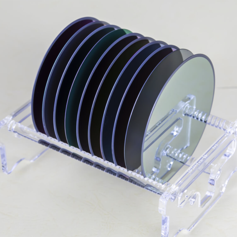
The 12inch BF33 substrate is a revolutionary new material that offers unparalleled performance and efficiency for semiconductor manufacturing. With its high thermal conductivity and superior electrical properties, the BF33 substrate is capable of delivering significant improvements in device performance, power consumption, and overall reliability. This breakthrough technology is poised to address the growing demand for high-performance semiconductors in a wide range of applications, including 5G communications, artificial intelligence, and automotive electronics.
The key advantage of the 12inch BF33 substrate lies in its ability to enhance the performance and efficiency of semiconductor devices. By enabling higher power densities and improved thermal management, the BF33 substrate allows for the development of highly efficient and reliable semiconductor products. This is particularly significant in the context of emerging technologies such as 5G, where the demand for high-speed, low-latency communication requires semiconductor devices to operate at unprecedented levels of performance.
In addition to its superior performance characteristics, the 12inch BF33 substrate also offers cost-effective benefits for semiconductor manufacturers. The use of BF33 substrate can result in higher production yields and lower overall manufacturing costs, making it an attractive solution for companies looking to maximize their operational efficiency and profitability. Furthermore, the scalability of the BF33 substrate makes it suitable for a wide range of semiconductor applications, from power devices to radio frequency (RF) components.
With the introduction of the 12inch BF33 substrate, {} is once again demonstrating its commitment to driving innovation and advancing the semiconductor industry. By leveraging their expertise in materials science and semiconductor manufacturing, the company is positioning itself as a leader in the development of advanced technologies that are shaping the future of electronics. As the demand for high-performance semiconductors continues to grow, the 12inch BF33 substrate is poised to play a vital role in meeting the evolving needs of the industry.
In conclusion, the 12inch BF33 substrate represents a major milestone in the advancement of semiconductor manufacturing. With its unmatched performance, efficiency, and cost-effective benefits, this groundbreaking material is set to redefine the capabilities of semiconductor devices and drive the next wave of technological innovation. As {} continues to lead the way in developing cutting-edge semiconductor solutions, the 12inch BF33 substrate stands as a testament to the company's commitment to pushing the boundaries of what is possible in the world of electronics.
Company News & Blog
How to Choose the Best Windows for Your Home: A Complete Guide
Sic Windows, a leading global provider of windows and doors, has recently announced the launch of a new line of energy-efficient products. This innovative range of windows is designed to meet the growing demand for sustainable and environmentally friendly building materials.With a strong focus on quality and sustainability, Sic Windows has established itself as a trusted and reliable provider of windows and doors for both residential and commercial projects. The company prides itself on its commitment to delivering high-performance products that not only enhance the aesthetic appeal of a building but also contribute to energy conservation and efficiency.The new line of energy-efficient windows is a testament to Sic Windows' dedication to innovation and sustainability. These windows are designed to minimize heat loss and reduce energy consumption, ultimately leading to lower heating and cooling costs for consumers. By incorporating advanced technologies and high-quality materials, Sic Windows has developed a range of products that not only meet industry standards but also exceed expectations in terms of performance and durability.In addition to their energy-efficient properties, these windows also boast a sleek and modern design, adding a touch of elegance to any building. With various styles and customizable options available, customers can choose the perfect windows to complement their architectural vision. Whether it's a contemporary residential project or a large-scale commercial development, Sic Windows' energy-efficient windows are the ideal choice for those looking to combine style and sustainability.Furthermore, Sic Windows is committed to reducing its environmental footprint throughout the production process. The company employs sustainable practices and utilizes recyclable materials to minimize waste and promote eco-friendly manufacturing. By prioritizing environmental stewardship, Sic Windows is not only setting the standard for energy-efficient windows but also leading the way in responsible and sustainable business operations.“We are thrilled to introduce our new line of energy-efficient windows to the market,” said [Company Spokesperson]. “At Sic Windows, we believe in delivering products that not only meet the needs of our customers but also contribute to a greener and more sustainable future. With our latest range of windows, we aim to provide a solution that combines cutting-edge technology with exceptional design, offering our customers the best of both worlds.”As the demand for energy-efficient building materials continues to grow, Sic Windows is well-positioned to meet the needs of the market. With a strong reputation for quality and reliability, the company's new line of windows is expected to make a significant impact in the construction and design industries. By providing a solution that prioritizes energy conservation and efficiency, Sic Windows is demonstrating its ongoing commitment to sustainability and innovation.Whether it's for a residential renovation project or a large-scale commercial development, Sic Windows' energy-efficient windows offer a compelling option for those looking to enhance their building's performance while reducing their environmental impact. With a focus on quality, sustainability, and innovation, Sic Windows is poised to lead the way in providing energy-efficient solutions for the modern building industry.
P Type Wafer Production to Witness Significant Growth in the Semiconductor Industry
P Type Wafer Continues to Revolutionize the Semiconductor IndustrySemiconductor technology has steadily grown over the years with the increasing reliance on electronic devices in our personal and professional lives. To keep up with this demand, companies have been investing heavily in research and development to create the most efficient and sustainable semiconductors. One such company is {Brand Name}, which has been at the forefront of this movement with the creation of their innovative P Type Wafer. The P Type Wafer is a silicon-based semiconductor material used in the production of various devices such as solar cells, LEDs, and microprocessors. Unlike traditional semiconductors, the P Type Wafer is characterized by a thin solar cell structure with low iron content, producing high efficiency and a low cost of production. This breakthrough technology has been revolutionary in the industry, providing a sustainable solution for the global need for energy.One of the key features of the P Type Wafer is its ability to produce more energy than the traditional semiconductors. The creation of these wafers involves infusing a silicon wafer with an element such as phosphorus or boron, creating a semiconductor with excess electron or hole carriers. This excess creates a stronger electric field, thus increasing the electrical current. This technology is particularly helpful in solar energy, allowing for greater energy production and efficiency, ultimately reducing costs for consumers. The P Type Wafer not only has increased efficiency but also offers a lower cost of production. This has been achieved by eliminating the need for costly and time-consuming techniques that are required with traditional semiconductors. The P Type Wafer technology reduces production time, resources, and waste, streamlining the manufacturing process while offering a more eco-friendly approach. {Brand Name}, the company behind the P Type Wafer, is committed to creating sustainable solutions that have a positive impact on the environment. Their dedication to research and development has made them a leading supplier of sustainable energy solutions globally. {Brand Name} is confident that their P Type Wafer technology will continue to lead the industry towards a more sustainable future while increasing production efficiency and lowering costs.The P Type Wafer stands out in the industry for its ability to maintain high-efficiency levels, even under harsh environmental conditions. These conditions include high-temperature, humidity, and irradiance. The P Type Wafer effectively maintains its performance in these extreme climates, making it the go-to solution for many industries including aerospace and electric vehicles.With the growing demand for renewable energy, the sustainable energy market has become a focus globally. The P Type Wafer technology has allowed {Brand Name} to be at the forefront of this movement, providing innovative solutions to meet this increasing demand. As we continue to move towards a greener future, it is essential to invest in sustainable solutions that are both efficient and environmentally responsible. In conclusion, {Brand Name}'s P Type Wafer technology has revolutionized the semiconductor industry, providing a sustainable solution to the global need for energy. Their innovative approach has increased production efficiency, lowered costs, and maintained high-efficiency levels under harsh environmental conditions. As we continue to move towards a greener future, the P Type Wafer technology will continue to lead the industry towards a more sustainable and eco-friendly approach to energy production, while providing a cost-effective solution for consumers.
Discover the Advantages of Gaas Substrate: A Breakthrough in Semiconductor Technology!
[Headline]: Groundbreaking Gaas Substrate Technology Revolutionizes the Semiconductor Industry[Subheadline]: An Introduction to the Company Leading the Transformation[Date][CITY], [STATE] - In an industry that is rapidly advancing and innovating, one company is at the forefront of a major breakthrough that is set to revolutionize the semiconductor industry. By developing and patenting a new Gallium Arsenide (GaAs) substrate technology, this company aims to enhance the performance and efficiency of electronic devices, paving the way for a new era of technological advancements.GaAs substrates have gained significant attention in recent years due to their unique properties and advantages over traditional silicon substrates. This cutting-edge technology enables the creation of devices that are highly efficient, compact, and capable of operating at high frequencies. With an ever-increasing demand for faster, more powerful electronic devices, GaAs substrates have become an attractive alternative to silicon.Leading the charge in GaAs substrate research and development is a pioneering company that has invested significant resources into realizing the full potential of this breakthrough technology. With a team of dedicated scientists, engineers, and researchers, this company has successfully developed a GaAs substrate that surpasses existing industry standards in terms of performance and functionality.One of the key advantages of this GaAs substrate technology relates to its ability to operate at higher frequencies with lower power consumption. This breakthrough ensures that electronic devices utilizing GaAs substrates are not only more energy-efficient but also capable of handling larger data loads. This will have far-reaching implications across a wide range of industries, including telecommunications, aerospace, and consumer electronics.Moreover, this company's GaAs substrate technology offers improved thermal management properties, meaning that devices can operate at higher temperatures without compromising their overall performance. This advancement is particularly crucial in applications such as wireless communication systems and high-speed data transfer, where maintaining signal integrity under extreme conditions is of utmost importance.In addition to these performance enhancements, this GaAs substrate technology also enables smaller device designs. By utilizing the superior conductivity and electron mobility properties of GaAs, electronic components can be made smaller without sacrificing performance. This not only leads to more compact and portable devices but also opens up new possibilities for wearable technology, Internet of Things (IoT) devices, and miniaturized medical devices.Given the immense potential of the GaAs substrate technology developed by this company, they are poised to disrupt the semiconductor industry and drive the next wave of technological advancements. By offering a viable alternative to silicon substrates, this technology ultimately empowers manufacturers to develop electronic devices that are faster, more efficient, and capable of meeting the growing demands of the market.As the global semiconductor industry continues to expand, the commercialization of GaAs substrate technology will undoubtedly play a pivotal role in shaping the future of electronic devices. The innovative efforts and groundbreaking accomplishments of this company represent a significant leap forward in the semiconductor industry, making them a key player in the upcoming era of technological transformation.With ongoing research and development and a commitment to continuous improvement, this company is set to solidify its position as a frontrunner in GaAs substrate technology. As the demand for advanced electronic devices continues to surge, the rapid commercialization of this revolutionary technology is not far off, promising a world where faster, smaller, and more energy-efficient devices reshape our lives.[Concluding paragraph:]In the years to come, the GaAs substrate technology developed by this company will undoubtedly disrupt the semiconductor industry, offering manufacturers and consumers alike a new frontier of possibilities. With its ability to enhance performance, reduce power consumption, and enable smaller device designs, this revolutionary technology is set to reshape the way we interact with electronic devices, catapulting us into a future where innovation knows no boundaries.
Advanced Semiconductor Company Develops Innovative InP Wafer for High-Performance Applications
Inp Wafer, a leading global semiconductor company specializing in the production of advanced silicon wafers, has recently made significant advancements in its manufacturing process that have garnered attention from industry experts and technology enthusiasts alike. The company's dedication to innovation and continuous improvement has led to a breakthrough in wafer technology that is set to revolutionize the semiconductor industry.Inp Wafer is known for its high-quality silicon wafers, which serve as the foundation for many electronic devices and microchips. These wafers are essential for the production of integrated circuits, memory chips, and other semiconductor components that are used in a wide range of applications, from consumer electronics to industrial machinery.The company's latest achievement comes in the form of a new and improved manufacturing process that promises to deliver even higher performance and efficiency in silicon wafer production. By utilizing cutting-edge technologies and industry-leading expertise, Inp Wafer has successfully optimized its manufacturing process to produce wafers with enhanced electrical and mechanical properties, paving the way for more advanced semiconductor devices with improved performance and reliability.Furthermore, Inp Wafer's dedication to sustainability and environmental responsibility has been a driving force behind its innovation efforts. The company has implemented eco-friendly practices and technologies in its manufacturing process, ensuring that its products are not only of the highest quality but also produced with minimal impact on the environment.Inp Wafer's commitment to research and development has been a key factor in its ability to stay at the forefront of the semiconductor industry. The company's team of scientists and engineers are constantly pushing the boundaries of what is possible in wafer technology, and their efforts have culminated in the latest breakthrough that is poised to set new standards for silicon wafer manufacturing.The implications of Inp Wafer's advancements in wafer technology are far-reaching. With the potential to improve the performance and efficiency of semiconductor devices, the new manufacturing process holds promise for a wide range of industries, from consumer electronics to automotive and beyond. Additionally, the company's focus on sustainability ensures that these advancements are made with a minimal environmental footprint, further enhancing their appeal in an increasingly eco-conscious market.Inp Wafer's latest achievement also serves as a testament to the company's commitment to delivering the highest quality products to its customers. With a reputation for excellence and a track record of innovation, Inp Wafer has solidified its position as a leading provider of silicon wafers for the semiconductor industry, and its latest breakthrough only further cements its status as a trailblazer in the field.As the semiconductor industry continues to evolve at a rapid pace, companies like Inp Wafer are at the forefront of driving innovation and pushing the boundaries of what is possible in semiconductor technology. With its latest advancements in wafer manufacturing, Inp Wafer is poised to shape the future of the industry and set new standards for performance, reliability, and sustainability.Inp Wafer's commitment to excellence, combined with its relentless pursuit of innovation, has positioned the company as a driving force in the semiconductor industry. As the company continues to push the boundaries of what is possible in wafer technology, it is clear that Inp Wafer is set to play a pivotal role in shaping the future of semiconductor devices and the technology that powers our world.
High-Quality 12-Inch Substrate for Electronic Devices
12inch BF33 Substrate: The Next Breakthrough in Semiconductor TechnologyIn the fast-paced world of semiconductor technology, the demand for more advanced and efficient substrates is constantly on the rise. With the continuous push for smaller, faster, and more powerful electronic devices, the development of innovative materials and processes has become paramount. In line with this, {Company Name}, a leading provider of advanced semiconductor solutions, has recently introduced the 12inch BF33 substrate, poised to be the next breakthrough in the industry.{Company Name} has been at the forefront of semiconductor innovation for over two decades, specializing in the development and production of cutting-edge materials and technologies. With a strong commitment to research and development, the company has consistently delivered high-quality solutions that have helped drive the advancement of various electronic applications.The 12inch BF33 substrate is the latest addition to {Company Name}'s extensive portfolio of semiconductor products, and it is set to revolutionize the industry with its exceptional performance and superior characteristics. The BF33 substrate is specifically designed to meet the growing demands of next-generation electronic devices, offering unparalleled precision, reliability, and efficiency.One of the key features of the 12inch BF33 substrate is its enhanced thermal and electrical properties, making it ideal for high-power and high-frequency applications. With its advanced thermal conductivity and low electrical resistance, the BF33 substrate is capable of handling the increasing power densities and frequencies in modern electronic systems, ensuring optimal performance and reliability.Furthermore, the 12inch BF33 substrate boasts excellent mechanical stability and chemical resistance, enabling it to withstand the stringent requirements of semiconductor manufacturing processes. Its exceptional uniformity and surface quality make it an ideal platform for the deposition of complex thin-film structures, providing a solid foundation for the fabrication of advanced semiconductor devices.In addition to its outstanding technical attributes, the 12inch BF33 substrate also offers significant cost benefits for semiconductor manufacturers. Its larger size and improved yield potential allow for greater efficiency and productivity in the production process, resulting in lower manufacturing costs and higher overall profitability.{Company Name} has invested heavily in the development and production of the 12inch BF33 substrate, leveraging its expertise and state-of-the-art manufacturing facilities to ensure the highest quality and consistency. The company's stringent quality control measures and rigorous testing procedures guarantee that the BF33 substrate meets the most demanding industry standards, providing customers with a reliable and high-performance solution for their semiconductor needs.As the demand for more advanced semiconductor materials continues to grow, the introduction of the 12inch BF33 substrate underscores {Company Name}'s commitment to pushing the boundaries of innovation and delivering cutting-edge solutions to the market. With its exceptional performance, reliability, and cost-effectiveness, the BF33 substrate is poised to set a new standard for semiconductor technology, driving the development of next-generation electronic devices and applications.In conclusion, the 12inch BF33 substrate represents a significant leap forward in semiconductor technology, offering a compelling combination of advanced technical capabilities and cost benefits. {Company Name} has once again demonstrated its leadership in the industry, showcasing its ability to develop and deliver groundbreaking solutions that address the evolving needs of the semiconductor market. As the demand for higher performance and more efficient electronic devices continues to escalate, the 12inch BF33 substrate stands ready to play a crucial role in shaping the future of semiconductor technology.
High-Quality Silicon Oxide Wafer: Everything You Need to Know
Silicon Oxide Wafer, a new product offered by a leading semiconductor company, is set to revolutionize the semiconductor industry with its cutting-edge technology. This innovative product is expected to have a significant impact on various sectors, including electronics, automotive, and healthcare.The Silicon Oxide Wafer is a crucial component in the manufacturing of semiconductor devices. It is a highly advanced material that offers superior performance and reliability compared to traditional wafers. The product is designed to meet the growing demand for high-quality semiconductor devices that can operate efficiently in a wide range of applications.The company behind this groundbreaking product has a solid reputation in the semiconductor industry. With several decades of experience in producing high-performance components, they have established themselves as a trusted supplier for many leading companies in the electronics and semiconductor sectors.The Silicon Oxide Wafer is the latest addition to the company's extensive portfolio of semiconductor products. It is the result of years of research and development, aimed at creating a material that can meet the evolving needs of the semiconductor industry. The company has invested heavily in state-of-the-art manufacturing facilities and cutting-edge technologies to ensure the highest quality standards for its products.One of the key advantages of the Silicon Oxide Wafer is its superior thermal and electrical properties. This enables semiconductor devices to operate at higher temperatures and with lower power consumption, making them ideal for a wide range of applications. Additionally, the wafer offers exceptional mechanical strength and reliability, ensuring that the semiconductor devices built on it can withstand harsh operating conditions.The company has also invested in developing environmentally friendly manufacturing processes for the Silicon Oxide Wafer. By using sustainable materials and energy-efficient production methods, they are committed to reducing their environmental impact and contributing to a more sustainable future for the semiconductor industry.The launch of the Silicon Oxide Wafer has generated significant interest within the semiconductor industry. Many leading companies have already expressed their intention to incorporate this innovative material into their semiconductor devices. This is expected to drive rapid adoption of the product across various applications, further solidifying the company's position as a key player in the semiconductor market.In addition to its technical capabilities, the Silicon Oxide Wafer is also expected to offer cost savings for semiconductor manufacturers. Its advanced properties can lead to higher yields and improved manufacturing efficiency, resulting in lower production costs and increased profitability for semiconductor companies.With the introduction of the Silicon Oxide Wafer, the company aims to strengthen its position as a leading provider of high-performance semiconductor materials. They are confident that this breakthrough product will help shape the future of the semiconductor industry and drive innovation in electronic devices, automotive systems, and healthcare technologies.The company is committed to continuing its investment in research and development to further advance the capabilities of the Silicon Oxide Wafer and other semiconductor products. By staying at the forefront of technological advancements, they aim to address the growing demands of the semiconductor industry and support the development of next-generation electronic devices.Overall, the launch of the Silicon Oxide Wafer represents a significant milestone for the semiconductor industry. With its advanced properties and potential for widespread adoption, this product is expected to have a transformative impact on various sectors, paving the way for the development of highly efficient and reliable semiconductor devices. The company's dedication to innovation and sustainability positions them as a key player in driving the future of the semiconductor industry.
Luxury Sapphire Crystal Watch Face: A Timepiece of Elegance and Durability
Luxury watch brand has recently unveiled their latest innovation in watch technology - the Sapphire Crystal Watch Face. This new watch face is set to revolutionize the industry with its advanced features and stunning design.The use of sapphire crystal in watch faces is not new, but this brand has taken it to the next level with their innovative approach. The sapphire crystal used in this watch face is not only highly scratch-resistant, but also incredibly clear and durable. This means that the watch face will remain pristine and free from scratches, even after years of wear.The design of the watch face is also a testament to the brand's commitment to excellence. The sleek and minimalist design is a perfect blend of form and function, with every detail carefully considered to provide the ultimate user experience. The sapphire crystal itself is elegantly framed by a stainless steel bezel, adding a touch of sophistication to the overall look of the watch.But what really sets this watch face apart is the advanced technology that has been integrated into it. The sapphire crystal is not just a protective layer, but also serves as a touch-sensitive interface for the watch. This means that users can easily navigate through the watch's features by simply tapping or swiping on the crystal. This not only adds a modern touch to the watch, but also makes it incredibly user-friendly.In addition, the sapphire crystal is also equipped with a high-resolution display that ensures the watch face is easy to read in any lighting conditions. Whether in bright sunlight or dimly lit environments, users can expect the watch face to remain perfectly legible at all times.This new innovation is a testament to the brand's commitment to pushing the boundaries of watchmaking. With a history of crafting timepieces that are not only luxurious, but also highly functional, this brand is always at the forefront of watch technology. The introduction of the Sapphire Crystal Watch Face is just another example of their dedication to innovation and excellence.The brand spokesperson commented, "We are thrilled to introduce the Sapphire Crystal Watch Face to our collection. It represents the culmination of years of research and development, and we believe it will set a new standard for luxury watches. Our goal has always been to create timepieces that are not only beautiful, but also practical, and we believe this new watch face achieves that and more."The Sapphire Crystal Watch Face is now available as part of the brand's latest watch collection. It is offered in a variety of styles and colors, ensuring that there is an option to suit every taste and preference. Whether it's paired with a classic leather strap or a sleek stainless steel bracelet, the Sapphire Crystal Watch Face is sure to make a statement on the wrist of any discerning watch enthusiast.In conclusion, the introduction of the Sapphire Crystal Watch Face is a significant milestone for the brand, further solidifying its position as a leader in luxury watchmaking. With its cutting-edge technology, stunning design, and unwavering commitment to quality, this new watch face is set to captivate watch enthusiasts around the world.
Delicious and Crispy Wafer Snacks: A New Favorite Street Food
Soi Wafer, a leading player in the semiconductor industry, has recently made waves with their cutting-edge wafer technology. With a focus on quality, innovation, and sustainability, Soi Wafer has become a trusted name in the industry, providing high-quality products to customers around the world.Established in [year], Soi Wafer has continuously pushed the boundaries of semiconductor technology, driving advancements in various applications such as automotive, consumer electronics, and industrial equipment. The company has built a solid reputation for delivering top-notch wafer solutions that meet the demands of an ever-evolving market.Soi Wafer's commitment to quality is evident in their state-of-the-art manufacturing facilities, which are equipped with the latest technology and operated by a team of skilled professionals. This allows the company to maintain stringent quality control measures throughout the production process, ensuring that each wafer meets the highest standards.In addition to quality, Soi Wafer is dedicated to driving innovation in the semiconductor industry. The company invests heavily in research and development, constantly seeking new ways to improve their wafer technology and stay ahead of the curve. This focus on innovation has led to the development of groundbreaking products that have set new benchmarks in the industry.But Soi Wafer's commitment to sustainability sets them apart from the competition. The company recognizes the environmental impact of semiconductor manufacturing and has implemented various initiatives to minimize their carbon footprint. From reducing energy consumption in their facilities to implementing eco-friendly production processes, Soi Wafer is dedicated to sustainable practices.Soi Wafer's recent achievement in wafer technology has garnered attention from industry experts and customers alike. The company's latest wafer, which boasts enhanced performance and reliability, has been praised for its potential to revolutionize various applications. This breakthrough has solidified Soi Wafer's position as a leader in the semiconductor market.The success of Soi Wafer can be attributed to their unwavering commitment to quality, innovation, and sustainability. By prioritizing these core values, the company has been able to deliver superior products that meet the needs of their customers while also contributing to a more sustainable future.Looking ahead, Soi Wafer shows no signs of slowing down. The company has ambitious plans for further expansion and diversification, with a strong focus on developing cutting-edge wafer technology that will shape the future of the semiconductor industry. With their track record of success and a clear vision for the future, Soi Wafer is poised to continue leading the way in semiconductor innovation.In conclusion, Soi Wafer's recent breakthrough in wafer technology is a testament to their unwavering commitment to excellence. With a focus on quality, innovation, and sustainability, the company has solidified its position as a trusted leader in the semiconductor industry. As Soi Wafer continues to push the boundaries of wafer technology, the future looks bright for this innovative company.
High-quality sapphire wafers for advanced technology applications
Sapphire wafers are changing the game in the technology world with their unique properties and applications. These wafers are made of sapphire, a crystalline form of aluminum oxide, and are increasingly being used in various industries for their exceptional durability and transparency.The use of sapphire in semiconductor manufacturing is growing rapidly due to its high thermal conductivity, electrical insulation, and resistance to wear and corrosion. This makes sapphire wafers an ideal material for applications such as LED production, consumer electronics, and industrial machinery.One company at the forefront of sapphire wafer production is a leading manufacturer in the semiconductor industry. With state-of-the-art facilities and a team of experts, they are able to produce high-quality sapphire wafers that meet the demanding requirements of their clients. These wafers are used in a wide range of applications, including advanced LED production, optical windows, and semiconductor components.Sapphire wafers are an essential component in the production of LEDs, which are becoming increasingly popular due to their energy efficiency and long lifespan. The unique properties of sapphire, such as its high light transmission and thermal conductivity, make it the material of choice for LED manufacturers. As the demand for LED lighting grows, so does the need for high-quality sapphire wafers, and this company is well-positioned to meet this growing demand.In addition to LED production, sapphire wafers are also used in consumer electronics, such as smartphones and tablets. The scratch-resistant nature of sapphire makes it an ideal material for protective screens, camera lenses, and other components that require durability and high optical quality. This company is a key supplier of sapphire wafers to the consumer electronics industry, providing their clients with the highest quality products for their devices.Furthermore, sapphire wafers are also used in industrial machinery and equipment, where durability and reliability are crucial. The high mechanical strength and chemical resistance of sapphire make it an excellent choice for applications such as bearings, seals, and other critical components. This company's sapphire wafers are used in a wide range of industrial applications, where they have earned a reputation for their exceptional performance and reliability.With their commitment to quality and innovation, this company is driving the advancement of sapphire wafer technology and expanding the possibilities for its use in various industries. Their continued investment in research and development ensures that they stay at the forefront of sapphire wafer production, providing their clients with cutting-edge solutions for their technical challenges.In conclusion, the use of sapphire wafers is revolutionizing the technology industry, and this company is playing a key role in this transformation. With their high-quality sapphire wafers and commitment to innovation, they are enabling their clients to push the boundaries of what is possible in LED production, consumer electronics, and industrial applications. As the demand for sapphire wafers continues to grow, this company is well-equipped to meet this demand and drive the future of sapphire technology.
Discover the Benefits of Silicon Carbide Polishing for a Flawless Finish
Silicon Carbide Polishing is a cutting-edge technique that has revolutionized the polishing industry. This method utilizes a combination of silicon carbide powder, water, and a polishing pad to produce a high-gloss finish on a variety of materials, including metals, plastics, and ceramics. The unique properties of silicon carbide make it an ideal material for polishing, as it is extremely hard and durable, allowing for precise and consistent results.One company that has made significant strides in the development of silicon carbide polishing is {}. The company was founded in the early 2000s and has since become a leader in the manufacturing and distribution of advanced polishing solutions. Their commitment to research and development has led to the creation of cutting-edge products that have set new standards in the industry. Their team of experts is dedicated to providing innovative solutions that meet the evolving needs of their customers.The company's silicon carbide polishing products have been widely recognized for their superior performance and reliability. Their proprietary formulation of silicon carbide powder ensures a consistent and uniform polishing action, resulting in a mirror-like finish. This level of precision is particularly valuable in industries such as aerospace, automotive, and electronics, where the quality of the finished product is of utmost importance.One of the key benefits of silicon carbide polishing is its ability to remove surface imperfections and create a smooth, uniform finish. This is essential for ensuring the optimum performance and longevity of components in various applications. Silicon carbide polishing also offers exceptional resistance to wear and tear, making it an ideal choice for high-traffic areas and components subject to heavy use.In addition to its superior performance, silicon carbide polishing is also environmentally friendly. Unlike traditional polishing methods that produce harmful emissions and waste, silicon carbide polishing is a clean and efficient process that minimizes the impact on the environment. This is an important consideration for companies looking to reduce their carbon footprint and operate sustainably.With the growing demand for high-quality surface finishes, the market for silicon carbide polishing is expected to expand significantly in the coming years. This presents an opportunity for companies like {} to further establish themselves as leaders in the industry. By continuing to invest in research and development, as well as maintaining a strong focus on customer satisfaction, they are well-positioned to capitalize on this growing trend.Furthermore, the company's commitment to innovation and excellence has earned them a strong reputation in the industry. They have built long-lasting relationships with a wide range of customers, from small businesses to multinational corporations, who rely on their expertise and products to achieve outstanding results. Their dedication to quality and customer service has set them apart from competitors and positioned them as a trusted partner in the industry.As the demand for silicon carbide polishing continues to grow, {} is poised to capitalize on this opportunity and further solidify their position as a leader in the industry. With their advanced products and commitment to excellence, they are well-equipped to meet the evolving needs of their customers and remain at the forefront of the industry.