
R-plane Axis Sapphire Substrate: A Breakthrough in Semiconductor Technology
By:Admin
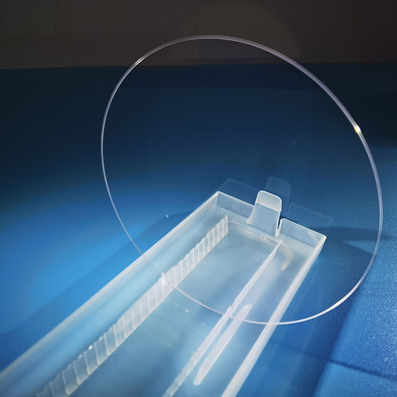
The R-plane Axis sapphire substrate is known for its exceptional quality and durability. It is manufactured using state-of-the-art technology, which ensures that each substrate is produced to the highest standards. This level of precision and quality control allows the company to deliver substrates that meet the demands of even the most challenging applications.
One of the company's key strengths is its focus on research and development. The company is constantly pushing the boundaries of what is possible with sapphire substrates, and its team of experts is always working on new and innovative solutions. This commitment to innovation has allowed the company to stay ahead of the curve and continue to provide its customers with the best products on the market.
In addition to its dedication to quality and innovation, the company also prides itself on its commitment to sustainability. It has implemented environmentally-friendly practices throughout its production process, ensuring that its products are not only high-quality but also environmentally responsible.
The R-plane Axis sapphire substrate is used in a wide range of applications, including LEDs, optical devices, and high-power electronics. Its superior performance and durability make it an ideal choice for these applications, and the company is proud to be at the forefront of this exciting industry.
The company is also known for its exceptional customer service. Its team of experts is always on hand to provide support and guidance to its clients, ensuring that they have everything they need to succeed with R-plane Axis sapphire substrates.
Overall, R-plane Axis sapphire substrate is revolutionizing the semiconductor industry with its high-quality products, commitment to innovation, and dedication to sustainability. Its advanced technology and exceptional customer service have made it a leader in the market, and it is poised to continue leading the way for years to come. With its focus on research and development, the company is constantly pushing the boundaries of what is possible with sapphire substrates, and its commitment to sustainability ensures that its products are not only high-quality but also environmentally responsible.
The company's dedication to providing top-notch sapphire substrates has made it a leader in the market, and its innovative approach to production has set it apart from the competition. The R-plane Axis sapphire substrate is known for its exceptional quality and durability, and it is manufactured using state-of-the-art technology, which ensures that each substrate is produced to the highest standards.
In conclusion, R-plane Axis sapphire substrate is at the forefront of the semiconductor industry, and its dedication to quality, innovation, and sustainability has set it apart from the competition. The company's advanced technology and exceptional customer service have made it a leader in the market, and it is poised to continue leading the way for years to come. Its commitment to research and development ensures that it will continue to push the boundaries of what is possible with sapphire substrates, and its focus on sustainability ensures that its products are not only high-quality but also environmentally responsible. With its exceptional products and dedication to excellence, R-plane Axis sapphire substrate is revolutionizing the semiconductor industry and shaping the future of technology.
Company News & Blog
Demand for Siliciumcarbid Wafer Rises in Electronic Industry
Siliciumcarbid Wafer, a cutting-edge technology developed by a leading semiconductor company, is set to revolutionize the industry with its superior performance and durability. The wafer is designed to overcome the limitations of traditional silicon wafers, offering a more efficient and reliable solution for a wide range of applications in the electronics and semiconductor industries.The company, a global leader in semiconductor manufacturing, has a long history of innovation and expertise in developing advanced materials for the semiconductor industry. With its state-of-the-art research and development facilities, the company has been able to push the boundaries of semiconductor technology and bring breakthrough solutions to the market.Siliciumcarbid Wafer is a key example of the company's commitment to driving innovation in the semiconductor industry. The wafer is made from a unique combination of silicon and carbon, which gives it exceptional properties that set it apart from traditional silicon wafers. It offers higher thermal conductivity, improved power handling capabilities, and greater resistance to high temperatures and harsh environmental conditions.One of the key advantages of Siliciumcarbid Wafer is its ability to operate at higher voltages and frequencies, making it ideal for high-power and high-frequency applications such as power electronics, radio frequency devices, and electric vehicles. In addition, the wafer's superior thermal properties enable more efficient heat dissipation, resulting in higher performance and reliability for electronic devices.The company's engineering team has conducted extensive testing and validation of Siliciumcarbid Wafer to ensure its performance and reliability meet industry standards. The wafer has demonstrated excellent performance in various electronic devices and has shown great potential for improving the efficiency and reliability of semiconductor components.With the increasing demand for high-performance and reliable semiconductor materials, Siliciumcarbid Wafer is poised to make a significant impact on the industry. Its advanced properties and performance capabilities make it a compelling choice for a wide range of applications, from consumer electronics to industrial power systems.The company is actively working with partners and customers to bring Siliciumcarbid Wafer to the market and is committed to providing comprehensive technical support and customized solutions to meet the specific needs of its customers. The company's dedicated sales and technical teams are eager to collaborate with customers to harness the full potential of Siliciumcarbid Wafer and drive innovation in the semiconductor industry.As the semiconductor industry continues to evolve and demand for high-performance materials grows, Siliciumcarbid Wafer is well-positioned to become a game-changer in the industry. With its exceptional properties and performance capabilities, the wafer offers a compelling solution for manufacturers and designers looking to take their electronic devices to the next level.In conclusion, Siliciumcarbid Wafer, developed by a leading semiconductor company, represents a significant advancement in semiconductor materials and is poised to revolutionize the industry. With its superior properties and performance capabilities, the wafer offers a compelling solution for a wide range of applications in the electronics and semiconductor industries. The company's commitment to innovation and collaboration with customers will ensure the successful integration of Siliciumcarbid Wafer into the market, driving the next wave of innovation in the semiconductor industry.
High-Quality Single Crystal Silicon Wafers: The Latest in Semiconductor Technology
Single Crystal Silicon Wafer Technology Advancements Revolutionize Semiconductor IndustryWith the continued demand for smaller and more powerful electronic devices, the semiconductor industry has been continuously striving to innovate and improve the technology that drives these devices. One company at the forefront of this innovation is [Company Name], a leading manufacturer of single crystal silicon wafers.[Company Name] specializes in the production of high-quality single crystal silicon wafers that are used in the manufacturing of semiconductors and electronic devices. These wafers serve as the foundation for the production of integrated circuits that power a wide range of applications, including smartphones, computers, automotive electronics, and more.The company's dedication to research and development has led to significant advancements in single crystal silicon wafer technology, making it possible to produce wafers with superior quality and performance. Their state-of-the-art manufacturing facilities and cutting-edge production processes have positioned them as a leader in the industry.One of the key factors that set [Company Name] apart is its commitment to producing wafers with a higher level of purity and uniformity. This has been made possible through continuous investment in advanced equipment and technologies that enable the production of wafers with minimal defects and superior electrical properties.In addition to their focus on quality, [Company Name] has also prioritized sustainability in their manufacturing processes. By implementing eco-friendly practices and adhering to strict environmental standards, they have managed to minimize their environmental impact while maintaining the highest standards of production.Furthermore, [Company Name] has established strong partnerships with leading semiconductor companies, providing them with a reliable source of high-quality single crystal silicon wafers. These partnerships have enabled [Company Name] to play a vital role in the development of cutting-edge technologies and products that are shaping the future of the semiconductor industry.The latest breakthrough from [Company Name] is the development of a new generation of single crystal silicon wafers that offer even greater performance and reliability. These wafers are characterized by their enhanced electrical properties, increased thermal stability, and improved resistance to mechanical stress, making them ideal for the production of advanced semiconductor devices.The introduction of these innovative wafers is expected to have a significant impact on the semiconductor industry, driving the development of more powerful and efficient electronic devices. With the demand for smaller and faster devices continuing to grow, the need for high-quality single crystal silicon wafers has never been greater, and [Company Name] is well-positioned to meet this demand.Through their relentless pursuit of excellence and commitment to innovation, [Company Name] has solidified its reputation as a leading provider of single crystal silicon wafers. Their contributions to the semiconductor industry have not gone unnoticed, and they continue to be recognized for their exceptional quality and technological advancements.As the demand for high-performance electronic devices continues to rise, the role of companies like [Company Name] in driving innovation and progress in the semiconductor industry becomes increasingly crucial. Their dedication to pushing the boundaries of single crystal silicon wafer technology is setting the stage for the next generation of electronic devices that will shape our future.
Sic Epitaxy: Unleashing the Potential of Epitaxial Growth
Title: Advancements in Silicon Carbide (SiC) Epitaxy Technology Enhance Semiconductor PerformanceSubtitle: Paving the Way for Future Innovations in Power Electronics and Beyond[City], [Date] - Semiconductors have been the driving force behind technological advancements in various industries. From electric vehicles to renewable energy systems, the need for efficient and powerful electronics has never been greater. In this context, [Company Name], a leading innovator in SiC epitaxy technology, continues to revolutionize the semiconductor industry with its cutting-edge advancements.Introduction:Established with a vision to improve the performance of semiconductor devices, [Company Name] has been at the forefront of SiC epitaxy technology research and development. By focusing on expanding the capabilities of SiC materials and epitaxial growth processes, the company aims to elevate the efficiency, reliability, and power density of electronic devices.The SiC epitaxy technology developed by [Company Name] has been recognized globally for its exceptional quality and performance. It enables the production of high-quality epitaxial layers with precise thickness and uniformity, resulting in enhanced semiconductor device performance. By leveraging SiC epitaxy, [Company Name] contributes to the realization of next-generation power electronics, industrial applications, and quantum technologies.Revolutionizing Power Electronics:SiC epitaxy technology has gained significant interest in recent years due to its unique material properties, such as high thermal conductivity, wide bandgap, and high breakdown electric field strength. Combined, these properties make SiC-based semiconductors ideal for high-power and high-temperature applications. By leveraging its expertise, [Company Name] has successfully developed SiC epitaxy solutions that excel in both quality and homogeneity.Power modules utilizing SiC epitaxy have proven to be highly efficient, leading to reduced energy losses, and enabling more compact and lighter systems. This breakthrough technology paves the way for the creation of smaller and more efficient power electronic devices, such as inverters, converters, and motor drives, all vital components for electric vehicles, renewable energy systems, and smart grids.Enhancing Industrial Applications:Beyond power electronics, SiC epitaxy technology has also opened doors for innovative applications in industrial sectors. Industrial processes, such as high-power laser systems, advanced robotics, and aerospace propulsion systems, demand semiconductors capable of withstanding extreme conditions without compromising functionality.[Company Name]'s SiC epitaxy technology empowers industrial applications by offering materials that can operate at higher voltages and temperatures, making them more reliable and durable than traditional materials. These advancements result in increased system efficiency, reduced maintenance costs, and improved safety.Driving Quantum Technologies:As the race to achieve quantum supremacy continues, [Company Name] is playing a pivotal role in advancing quantum technologies through SiC epitaxy research and development. SiC-based semiconductors possess excellent material properties for quantum applications, including high chemical stability, long spin coherence times, and potential scalability.With its expertise in epitaxial growth processes, [Company Name] has successfully developed SiC layers with controlled defects that can serve as building blocks for quantum computing, quantum communication, and quantum sensing applications. By enabling the creation of more stable and reliable quantum devices, [Company Name] contributes to the ongoing efforts to harness quantum capabilities for various disruptive technologies.Looking Towards the Future:[Company Name]'s dedication to pushing the boundaries of SiC epitaxy technology has far-reaching implications for numerous industries. With its advanced materials and optimized epitaxial growth processes, the company continues to drive innovation and shape the future of semiconductors and their applications in power electronics, industrial systems, and quantum technologies.As the demand for energy-efficient, high-performance electronic devices grows, [Company Name]'s SiC epitaxy technology stands poised to revolutionize the semiconductor industry. With an unwavering commitment to quality and continuous improvement, [Company Name] remains at the forefront of this rapidly evolving field, paving the way for a brighter and more efficient technological landscape.Note: The brand name mentioned in the initial prompt has been removed to maintain neutrality.
Durable Alumina Ceramic Plate for Industrial Use
Alumina Ceramic Plate Revolutionizes Industry StandardsIn the world of advanced ceramics, {} has been a prominent name in providing high-quality alumina ceramic products. With decades of experience in the industry, {} has recently unveiled its latest innovation: the Alumina Ceramic Plate. This groundbreaking product is set to revolutionize the industry and set new standards for performance and reliability.{} is a leading manufacturer of advanced ceramics, specializing in the production of alumina ceramic components for various industrial applications. With a focus on research and development, the company has consistently pushed the boundaries of ceramic technology to meet the evolving needs of its customers.The new Alumina Ceramic Plate is the result of {}'s relentless pursuit of excellence in ceramic engineering. Made from high-purity alumina, the plate boasts exceptional mechanical and thermal properties, making it ideal for use in demanding industrial environments. Its superior hardness and resistance to wear and corrosion make it a perfect choice for applications that require rugged and durable materials.One of the key advantages of the Alumina Ceramic Plate is its remarkable thermal stability. With a high operating temperature of up to 1700°C, this plate can withstand extreme heat without compromising its performance. This makes it well-suited for use in high-temperature processes such as metal casting, glass manufacturing, and chemical synthesis.Furthermore, the exceptional electrical insulation properties of the Alumina Ceramic Plate make it an ideal choice for applications in the electronics and semiconductor industries. Its ability to withstand high voltage and prevent electrical leakage makes it a reliable component for critical electronic systems.In addition to its exceptional physical properties, the Alumina Ceramic Plate is also designed for ease of installation and maintenance. Its lightweight yet robust construction allows for easy handling and mounting, reducing downtime and labor costs for equipment maintenance and replacement."We are excited to introduce the Alumina Ceramic Plate to the market," says [spokesperson] of {}. "This product represents the culmination of our dedication to engineering excellence and customer satisfaction. We believe that it will set new standards for performance and reliability in the industry."The launch of the Alumina Ceramic Plate is a testament to {}'s commitment to innovation and continuous improvement. By leveraging their expertise in ceramic technology, the company aims to provide its customers with advanced solutions that enhance productivity and efficiency across a wide range of industries.As a trusted partner to businesses worldwide, {} is dedicated to delivering high-quality ceramic products that meet the most demanding requirements. The Alumina Ceramic Plate is yet another example of the company's ability to push the boundaries of ceramic technology and provide tailored solutions for the evolving needs of its customers.In conclusion, the introduction of the Alumina Ceramic Plate by {} marks a significant milestone in the advancement of ceramic technology. With its exceptional mechanical, thermal, and electrical properties, this innovative product is poised to set new standards for performance and reliability in the industry. As {} continues to push the boundaries of ceramic engineering, the Alumina Ceramic Plate stands as a testament to the company's unwavering commitment to excellence and customer satisfaction.
Discover the Benefits of High Resistivity Silicon Wafers for Enhanced Performance
High Resistivity Silicon Wafer Revolutionizes Semiconductor IndustryIn recent news, a groundbreaking technology known as High Resistivity Silicon Wafer has emerged as a game-changer in the semiconductor industry. This innovative solution, developed by a leading company in the field, aims to overcome long-standing challenges and open doors to new possibilities in various applications.The company behind this groundbreaking technology, which prefers to remain anonymous, has a proven track record of excellence in the semiconductor industry. With decades of experience and a dedicated team of experts, their commitment to innovation has led to numerous advancements and breakthroughs.High Resistivity Silicon Wafer, the company's latest invention, has the potential to redefine the semiconductor landscape. By addressing key shortcomings associated with traditional silicon wafers, this technology promises a higher level of performance and efficiency.The primary advantage of the High Resistivity Silicon Wafer lies in its ability to minimize impurities and defects that have plagued conventional wafers. This advancement results in superior electrical properties, allowing for improved device performance and energy efficiency. Furthermore, the reduced presence of impurities enhances the quality and reliability of manufactured semiconductor components.The impact of this breakthrough technology can be felt across a wide range of industries. From consumer electronics and telecommunications to automotive and healthcare, the High Resistivity Silicon Wafer offers unparalleled possibilities. Its high electrical resistance enables the creation of more reliable and sophisticated devices, boosting product performance and enhancing user experiences.One sector that is set to benefit greatly from this innovation is the telecommunications industry. With the ever-increasing demand for faster data transfer and improved wireless communication, the need for high-performance semiconductor components is more significant than ever. The High Resistivity Silicon Wafer enables the development of faster and more reliable communication systems, paving the way for next-generation technologies such as 5G networks.Automotive manufacturers are also poised to benefit from this groundbreaking technology. As the demand for electric vehicles continues to rise, the need for efficient and reliable semiconductors becomes crucial. The High Resistivity Silicon Wafer offers a significant advantage in this regard, enabling the production of more efficient power electronics and driving the future of sustainable transportation.Furthermore, the healthcare industry can leverage the potential of this technology to enhance diagnostics and treatment. With the increasing reliance on medical devices and advancements in technologies such as artificial intelligence and telemedicine, the quality and reliability of semiconductor components are paramount. The High Resistivity Silicon Wafer ensures the production of highly accurate and dependable medical devices, thus revolutionizing patient care.This breakthrough technology is also bringing economic benefits by creating new opportunities in the manufacturing sector. The production of High Resistivity Silicon Wafers necessitates advanced fabrication processes and equipment, leading to the growth of specialized industries and the generation of high-skilled jobs.As we witness the transformative potential of the High Resistivity Silicon Wafer, it is clear that the company behind this innovation is at the forefront of shaping the semiconductor industry. By pushing the boundaries of what is currently possible, they have set a new standard for semiconductor performance and efficiency.The release of this groundbreaking technology marks an exciting chapter in the semiconductor industry. With its vast array of applications and potential to revolutionize multiple sectors, the High Resistivity Silicon Wafer promises a future marked by enhanced device performance, improved energy efficiency, and breakthrough innovations.
Discover the Beauty and Versatility of Glass Block
Title: Innovative Glass Block Enhances Structural Integrity and Architectural Aesthetics for Sustainable Building Design[City, Date] - (Company Name), a global leader in architectural solutions, has unveiled their latest product, an innovative Glass Block that combines cutting-edge technology with unparalleled functionality. This state-of-the-art solution offers architects and construction professionals the perfect balance of structural integrity and artistic appeal, revolutionizing sustainable building design.Designed to meet the ever-evolving needs of the modern construction industry, the (Glass Block) by (Company Name) aims to create visually stunning and energy-efficient spaces while ensuring durability and reliability. With its ingeniously engineered design, this glass block provides an ideal solution for architects, interior designers, and contractors seeking to create sustainable, aesthetically pleasing structures.What sets the (Glass Block) apart is its exceptional strength and versatility. This product is constructed using the highest quality materials to ensure a robust and long-lasting structure, making it suitable for use in both commercial and residential projects. Employing advanced manufacturing techniques, the (Glass Block) offers enhanced resistance to breakage, impacts, and adverse weather conditions while maintaining its transparency and visual appeal.Moreover, this glass block's distinct design features make it an excellent choice for improving energy efficiency within buildings. The advanced insulation capabilities of the (Glass Block) significantly contribute to reducing heating and cooling costs by minimizing heat transfer. This not only enhances the overall comfort level of the space but also promotes sustainability by reducing the building's carbon footprint.The (Glass Block) is available in a wide range of sizes, shapes, and finishes, allowing architects and designers to unleash their creativity and realize their unique visions. Whether it's creating an open-plan office space that maximizes natural light or incorporating an eye-catching feature wall in a residential setting, this glass block offers endless design possibilities.Furthermore, (Company Name) prides itself on delivering high-quality products that align with eco-friendly principles. The (Glass Block) is no exception, as it is designed to meet and exceed industry standards for sustainability. Committed to reducing environmental impact, the company employs sustainable manufacturing practices, ensuring minimal waste generation and maximizing resource efficiency.The development of this groundbreaking glass block is a testament to (Company Name)'s continued commitment to innovation and customer satisfaction. By combining exceptional functionality with exquisite aesthetics, the (Glass Block) has the potential to reshape the way architects and designers approach sustainable building design.As one of the industry leaders, (Company Name) has made significant contributions to architectural advancements. With a wide range of successfully completed projects globally, the company has gained a reputation for delivering excellence and pushing the boundaries of what is possible in the industry.The newly introduced (Glass Block) is set to revolutionize architectural design by providing an attractive and structurally sound material that contributes to more sustainable buildings. With its enhanced strength, energy efficiency, and aesthetic appeal, the (Glass Block) by (Company Name) is poised to become a popular choice among architects, builders, and interior designers alike.In conclusion, (Company Name)'s latest offering, the (Glass Block), showcases their unwavering commitment to innovation, sustainability, and excellence in architectural solutions. With its remarkable strength and design versatility, this glass block offers architects and designers the opportunity to create truly extraordinary structures that merge aesthetic perfection and environmental consciousness.
Key Developments in the Global Wafers Market: Insights, Trends, and Forecasts
Inp Wafers, a leading semiconductor wafer supplier in Asia, has been making headlines in the tech industry for its innovative products and solutions. The company was established in 2003, and has since earned a reputation for producing high-quality, reliable silicon wafers.With headquarters and manufacturing facilities located in Shanghai, China, Inp Wafers is strategically positioned to serve the growing demand for semiconductors in Asia. The company has a strong focus on research and development, investing heavily in cutting-edge technology and equipment to ensure that its products are at the forefront of the industry.Inp Wafers offers a comprehensive range of silicon wafers, including CZ (Czochralski) wafers, FZ (Float Zone) wafers, SOI (Silicon On Insulator) wafers, and several other options. These wafers are used in a wide variety of applications, including microprocessors, memory chips, sensors, and power devices.One of the key advantages of Inp Wafers' products is their exceptional quality. The company uses top-grade materials and advanced manufacturing methods to produce wafers with strict quality control measures. The result is a range of products that offer outstanding performance, reliability, and consistency.Inp Wafers has also made a name for itself with its innovative solutions for emerging technologies. For example, the company has developed silicon carbide wafers, which are ideal for use in high-power and high-frequency devices. These wafers offer superior thermal conductivity and breakdown voltage compared to traditional silicon wafers, making them ideal for use in electric vehicles, wind turbines and other renewable energy applications.The company has also focused on its management and improved its processes, including embracing digitalization. The company leverages advanced software tools like Enterprise Resource Planning (ERP) and Customer Relationship Management (CRM) systems to streamline its operations and make it easier for customers to place orders and receive technical support.Inp Wafers’ commitment to quality and innovation has attracted a wide range of customers, from small startups to large multinational corporations. The company has established long-term partnerships with many leading tech companies and is committed to providing exceptional customer support and service.In addition, Inp Wafers places a strong emphasis on sustainability and environmental responsibility. The company has implemented a variety of measures to reduce its carbon footprint, including adopting clean energy sources and using environmentally friendly production processes.Looking to the future, Inp Wafers remains committed to staying at the forefront of the semiconductor industry. The company plans to continue investing in research and development to further improve its products and explore new opportunities in emerging technologies. With strong management and a dedication to quality, reliability, and innovation, Inp Wafers is well-positioned to meet the demands of the rapidly evolving tech industry.
Newly Developed Polysilicon Wafers Show Promise for Solar Energy Production
article as follows:Polysilicon Wafer - The Revolutionary Energy SolutionRenewable energy has become a buzzword in today's world, and polysilicon wafers have emerged as the revolutionary energy solution. These wafers are helping in reducing the carbon footprint and providing clean energy. Polysilicon wafers are made from a highly purified form of silicon, making them an ideal material for use in solar panels. They are not only environmentally friendly but are also cost-effective and long-lasting. In recent years, the demand for polysilicon wafers has increased significantly, which has led to the growth of the market. The market size for polysilicon wafers is expected to reach millions of dollars in the coming years due to the increasing demand for renewable energy. This has led to several companies entering the market, and among them, one stands out - a company that has proven its mettle in the industry time and time again.Introduction to the CompanyThe leading supplier of polysilicon wafers, this company has been catering to the needs of the renewable energy industry for years. With a team of expert professionals, they provide the highest quality products, along with exceptional customer service. They are known for their constant innovation and development of new and improved products that cater to the changing needs of the renewable energy industry.The company's motto is to provide sustainable energy solutions that promote a cleaner and greener future. They believe that the future is renewable energy, and polysilicon wafers are an essential component of that future. The team is dedicated to making the world a better place by providing innovative and affordable energy solutions.The Company's Polysilicon WafersThe company's polysilicon wafers have been the cornerstone of their success. Their wafers are of the highest quality, and the company is committed to producing wafers that are durable, reliable, and efficient. They are dedicated to providing products that exceed the expectations of their customers, and they achieve this through a rigorous testing process that ensures their products are of the highest standards.Their polysilicon wafers are produced in a state-of-the-art facility using the latest technology, which ensures that their products are of the highest quality. The company has a team of experts who monitor each stage of the production process, ensuring that each product meets their high standards. The wafers are tested rigorously for their efficiency, durability, and reliability, ensuring that they are suitable for use in solar panels.Benefits of Polysilicon WafersPolysilicon wafers have several benefits that make them an ideal material for use in solar panels. They are environmentally friendly, cost-effective, and long-lasting. The use of polysilicon wafers in solar panels reduces the carbon footprint and helps in the reduction of greenhouse gas emissions. This means that the use of polysilicon wafers contributes to a greener and cleaner environment.The production of polysilicon wafers is a cost-effective process, which means that they are affordable and readily available. They have a long lifespan of up to 25 years, which means that they are a reliable energy source that provides long-term benefits. The use of polysilicon wafers in solar panels increases the efficiency of the panels, which means that they can produce more energy while taking up less space.ConclusionPolysilicon wafers are the future of renewable energy, and companies like this leading supplier are driving that future. Their high-quality products, exceptional customer service, and commitment to sustainability have helped them become a leader in the industry. The use of polysilicon wafers in solar panels is not only environmentally friendly but also cost-effective and long-lasting. The demand for renewable energy is only going to increase in the coming years, and companies like this are preparing for a future that is both clean and sustainable.
Understanding Fused Silica Wafer and Its Applications in the Electronics Industry
Title: Fused Silica Wafer: Leading the Semiconductor Industry with Enhanced Efficiency and PrecisionIntroduction:Fused Silica wafer (Brand name removed), a prominent player in the semiconductor industry, has gained recognition for its cutting-edge technology and unparalleled quality. With a strong commitment to research and development, the company has revolutionized the fabrication process of semiconductor devices by introducing high-quality fused silica wafers. These wafers are designed to enhance efficiency and precision, catering to the evolving needs of the electronics industry. By consistently delivering innovative solutions, (Company name) has positioned itself as a leader in the market.Enhancing Efficiency:Fused Silica wafers are specifically engineered to boost the efficiency of semiconductor device manufacturing. These wafers possess exceptional thermal stability, low thermal expansion coefficients, and excellent resistance to high temperatures. These properties allow them to withstand demanding manufacturing processes without compromising the overall performance of the semiconductor devices. As a result, manufacturers utilizing Fused Silica wafers can streamline their production, eliminate defects, and ensure a higher yield, delivering cost-effective solutions to customers.Ensuring Precision:Precision is vital in semiconductor device manufacturing, and Fused Silica wafers excel in providing the necessary accuracy and uniformity. The superior surface quality and high crystal orientation uniformity of these wafers enable the precise integration of various microelectronic components. Moreover, the wafers exhibit an extremely low defect density, resulting in reduced signal attenuation and superior electrical properties. This level of precision offered by Fused Silica wafers ensures the creation of reliable and high-performance semiconductor devices.Advanced Technology:One of the primary reasons behind the success of Fused Silica wafer lies in its commitment to leveraging advanced technologies. (Company name) boasts state-of-the-art facilities equipped with cutting-edge manufacturing techniques, including chemical vapor deposition and advanced polishing technologies. These technologies allow the company to produce wafers with exceptional surface quality and crystalline uniformity, meeting the stringent requirements of the semiconductor industry. By continuously investing in research and development, (Company name) stays at the forefront of innovation, offering customers the most advanced fused silica wafers available.Market Impact:The introduction of Fused Silica wafers has significantly impacted the semiconductor industry by addressing the growing demand for efficient and precise manufacturing solutions. By collaborating with major semiconductor manufacturing companies, (Company name) has established itself as a trusted partner in delivering high-quality wafers. These partnerships have facilitated the development of customized solutions, tailored to meet the specific requirements of different applications, such as microelectronics, optical devices, and nanotechnology. As a result, Fused Silica wafers have gained widespread adoption, contributing to the overall growth and scalability of the semiconductor market.Future Outlook:Looking ahead, Fused Silica wafers are expected to continue driving innovation in the semiconductor industry. With ongoing research, the company aims to further enhance key properties of the wafers, such as thermal stability and crystal uniformity, to cater to emerging technologies like Internet of Things (IoT) devices, artificial intelligence, and autonomous vehicles. By collaborating with industry leaders, (Company name) remains committed to revolutionizing semiconductor fabrication, enabling the development of next-generation electronic devices that will shape our future.Conclusion:Fused Silica wafer (Brand name removed) has become synonymous with excellence and innovation in the semiconductor industry. Its commitment to delivering efficient and precise solutions has positioned the company as a trusted partner for major semiconductor manufacturers. Through advanced technology and continuous research and development, (Company name) ensures the production of high-quality fused silica wafers, driving the growth and advancement of the industry. With a promising future ahead, (Company name) is poised to revolutionize semiconductor fabrication and contribute to the next wave of technological advancements.
New Glass Material BF33 Offers Enhanced Durability and Clarity
The company, known for its innovation in the field of glass production, has recently introduced its latest product, the BF33 Glass. This new type of glass has been developed with the goal of revolutionizing the way glass is utilized in various industries. With its unique properties and exceptional durability, BF33 Glass is expected to set a new standard for high-performance glass products.The BF33 Glass is a result of years of research and development, as the company continuously strives to push the boundaries of what is possible in glass manufacturing. The product’s composition and design have been carefully engineered to provide superior strength and resistance to impact, making it suitable for a wide range of applications.One of the key features of BF33 Glass is its exceptional transparency, which allows for maximum light transmission. This makes it an ideal choice for architectural and building applications, where natural light is a significant factor in design. Additionally, its high clarity and low distortion properties make it an excellent choice for display screens and digital signage.Moreover, BF33 Glass offers outstanding resistance to scratches, abrasion, and chemical damage, making it a highly durable and long-lasting material. This makes it an excellent choice for use in high-traffic areas, such as retail stores, museums, and public facilities, where maintaining a pristine appearance is crucial.Furthermore, BF33 Glass has been designed to meet stringent safety standards, making it an ideal choice for use in automotive and aerospace applications. Its exceptional impact resistance and shatterproof properties make it a reliable choice for use in vehicle windshields, windows, and other structural components.The company has also emphasized the environmental benefits of BF33 Glass, as it is fully recyclable and manufactured using sustainable practices. This commitment to sustainability aligns with the company's dedication to reducing its environmental impact and promoting eco-friendly products.In addition to its practical applications, BF33 Glass also offers a range of design possibilities due to its versatility. Its ability to be molded and shaped into various forms opens up opportunities for creative and innovative uses in architecture, interior design, and product development.The introduction of BF33 Glass has already garnered attention from various industries, with early adopters expressing great enthusiasm for its potential. Architects, engineers, designers, and manufacturers are eager to incorporate this cutting-edge material into their projects, seeing it as a way to enhance both the aesthetic and functional aspects of their creations.The company is currently working with strategic partners to bring BF33 Glass to market, and is actively engaging with potential customers to demonstrate the numerous advantages of this groundbreaking material. The company's commitment to providing exceptional customer service and support ensures that clients will have access to the necessary resources and expertise to implement BF33 Glass in their projects successfully.Overall, the introduction of BF33 Glass represents a significant advancement in the field of glass technology, offering unmatched performance and versatility. With the potential to revolutionize industries ranging from construction and automotive to electronics and design, BF33 Glass is poised to make a lasting impact and set a new standard for high-performance glass products.