
Sapphire Wafer for C-plane Axis: Recent Developments and Advancements
By:Admin
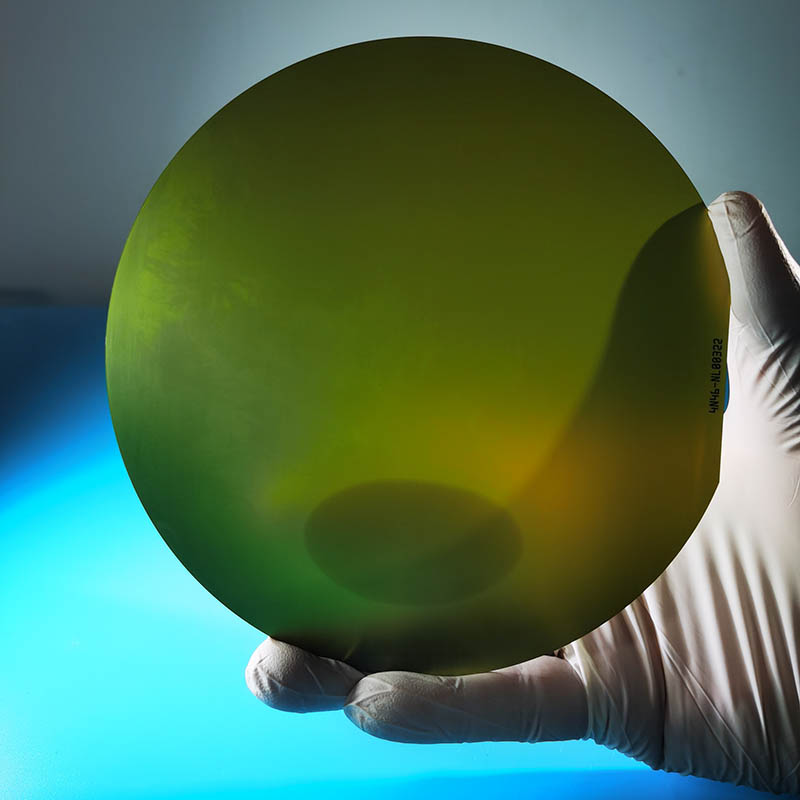
Sapphire is a highly versatile material that has become widely used in various industries, including semiconductor, aerospace, and defense. Its unique properties, such as high thermal conductivity, high strength, and optical transparency have made it an ideal material for applications that require high performance and reliability.
A leading manufacturer in the sapphire substrate technology industry, C-plane Axis, has been at the forefront of developing high-quality sapphire wafers for a wide range of applications. Their innovative C-plane Axis sapphire wafer has set a new standard in the industry, offering unmatched performance and reliability.
The company's C-plane Axis sapphire wafer is a result of years of research and development, and it represents a significant advancement in sapphire substrate technology. The wafer is produced using a proprietary process that ensures the highest level of quality and consistency. This process allows for precise control over the wafer's crystalline structure, which is essential for achieving superior mechanical and optical properties.
One of the key features of the C-plane Axis sapphire wafer is its exceptional flatness and surface finish. This allows for better bonding and integration with other materials, making it an ideal choice for use in advanced semiconductor devices. The wafer also exhibits excellent optical clarity, making it suitable for applications in high-power LEDs, optical windows, and lenses.
In addition to its superior physical properties, the C-plane Axis sapphire wafer also offers excellent thermal conductivity, which is critical for applications in high-power electronics and RF devices. The wafer's high thermal conductivity enables efficient heat dissipation, contributing to the overall performance and reliability of the devices in which it is used.
Furthermore, the C-plane Axis sapphire wafer is available in a wide range of sizes and thicknesses, making it suitable for various manufacturing processes and applications. This flexibility allows for greater design freedom and customization, meeting the specific requirements of different industries and applications.
Aside from its technical specifications, the C-plane Axis sapphire wafer is also produced with an environmentally friendly approach. The manufacturing process minimizes waste and energy consumption, aligning with the company's commitment to sustainability and responsible manufacturing practices.
The C-plane Axis sapphire wafer has garnered international recognition and has been adopted by leading companies in the semiconductor, aerospace, and defense industries. Its superior performance and reliability have made it the preferred choice for demanding applications that require the highest level of quality and performance.
C-plane Axis, the company behind the innovative sapphire wafer, is a global leader in sapphire substrate technology. With a strong focus on research and development, the company continues to push the boundaries of sapphire material science, driving innovation and excellence in the industry.
Established in [year], C-plane Axis has built a solid reputation for delivering high-quality sapphire wafers that meet the stringent requirements of various industries. The company's state-of-the-art manufacturing facilities and advanced process technologies enable them to produce sapphire wafers with exceptional precision and performance.
In addition to their cutting-edge products, C-plane Axis is committed to providing unparalleled customer support and technical expertise. Their team of highly skilled engineers and researchers work closely with customers to develop customized solutions that address their specific needs and requirements.
As the demand for high-performance materials continues to grow, C-plane Axis remains dedicated to driving innovation and setting new standards in sapphire substrate technology. The company's C-plane Axis sapphire wafer stands as a testament to their commitment to excellence and their ability to deliver superior products that meet the evolving needs of the industry.
In conclusion, the C-plane Axis sapphire wafer represents a significant advancement in sapphire substrate technology, offering unmatched performance and reliability for a wide range of applications. With its superior physical properties, environmentally friendly manufacturing process, and exceptional technical support, C-plane Axis continues to lead the industry in sapphire material science, driving innovation and excellence in the field.
Company News & Blog
Unlocking the Potential of Silica Sio2: Breaking Down Its Importance and Applications
article.Silica SiO2 – Revolutionizing the Construction IndustrySilica SiO2 (need remove brand name) is a revolutionary product that has created a buzz in the construction industry. It is a high-performance additive that enables the production of high-quality concrete. This advanced material enhances the strength and durability of concrete structures, making them more resistant to weathering and wear.Silica SiO2 is created through a unique manufacturing process, which involves extracting and purifying silica from raw materials such as sand, quartz, and shale. This specialized process produces a pure form of silica, which is then processed into a fine powder. The product is carefully formulated with a blend of other minerals, which work synergistically to provide better performance.The use of Silica SiO2 in the construction industry is gaining more popularity due to its superior properties. This innovative material is specifically designed to improve the quality of concrete by enhancing its compressive, tensile, and flexural strength. It also improves the durability of concrete structures, enabling them to withstand harsh weather conditions and heavy traffic loads.Silica SiO2 is easy to use and is suitable for all types of concrete mixes, including ready-mix, precast, and shotcrete. It can be added to the mix during the batching process or can be included as a standalone ingredient. The product is compatible with all types of cement and does not affect the concrete drying time.One of the significant benefits of Silica SiO2 is that it reduces the amount of carbon dioxide emissions in the atmosphere. Concrete production is one of the leading contributors to CO2 emissions, and Silica SiO2 helps to reduce the carbon footprint of concrete structures. By enabling the use of high-quality concrete with enhanced properties, Silica SiO2 facilitates the construction of more eco-friendly and sustainable buildings.The benefits of Silica SiO2 are not limited to concrete properties alone. It also enhances the workability of the mix, making it easier to place and finish. It reduces the risk of segregation and bleeding, which can compromise the quality of the concrete. Furthermore, Silica SiO2 helps to reduce water permeability, thus improving the overall water resistance of the structure.Silica SiO2 is a product that is backed by extensive research and development. The manufacturers of Silica SiO2 conduct rigorous testing to ensure that the product meets and exceeds industry standards. Silica SiO2 is tested for various aspects, including its strength, durability, compatibility, and environmental impact. The results of these tests demonstrate the superior properties of Silica SiO2, making it a reliable and trustworthy product.In conclusion, Silica SiO2 is an innovative material that is revolutionizing the construction industry. It is a high-performance additive that enhances the quality of concrete structures by improving their strength, durability, and sustainability. With increasing demand for eco-friendly and sustainable buildings, Silica SiO2 is emerging as the go-to solution for construction professionals who want to improve the quality of their concrete structures while reducing their environmental footprint. Silica SiO2 is a product that is here to stay, and its application in concrete is only expected to increase in the coming years.
Discover the Latest Advancements in Wafer Window Technology
Mgo Wafer Windows Revolutionize the Window Industry[Company Name], a leading innovative materials technology company, has recently introduced a revolutionary product that is set to transform the window industry. Mgo Wafer Windows, a groundbreaking development in window technology, promise increased durability, enhanced thermal insulation, and improved soundproofing. With their innovative design and advanced properties, these windows are poised to become the go-to choice for architects, builders, and homeowners alike.Traditional windows have long been plagued by issues such as susceptibility to damage, limited insulation capabilities, and poor soundproofing. [Company Name] recognized these pain points and embarked on a mission to develop a solution that would alleviate these problems. The result of their relentless research and development efforts is the Mgo Wafer Windows – a product that promises to revolutionize the way we think about and experience windows.One of the key advantages of Mgo Wafer Windows is their exceptional durability. Unlike traditional windows, which are prone to cracks, discoloration, and warping over time, Mgo Wafer Windows are composed of magnesium oxide, a material known for its high strength and resistance to wear and tear. This superior durability ensures that the windows retain their aesthetic appeal and functionality for extended periods, saving homeowners from the hassle and cost of regular replacements.Furthermore, Mgo Wafer Windows excel in thermal insulation, offering a significant improvement over conventional windows. These windows feature advanced insulation properties that minimize heat transfer, resulting in reduced energy consumption for heating or cooling buildings. As a result, homeowners can enjoy a more comfortable and energy-efficient living environment while simultaneously reducing their carbon footprint.Another area where Mgo Wafer Windows shine is soundproofing. The advanced design of these windows incorporates multiple layers of sound-dampening materials, effectively reducing noise pollution from outside sources. This is particularly beneficial for urban areas, where excessive noise can negatively impact the quality of life. Mgo Wafer Windows provide the peace and tranquility that homeowners desire, allowing them to relax and unwind without disturbances.Additionally, Mgo Wafer Windows offer an array of customizable options, ensuring they seamlessly blend with various architectural styles. Homeowners and architects can choose from a wide range of sizes, shapes, and designs to meet their unique preferences and requirements. This versatility allows for creativity in design and enhances the overall aesthetics of any building or space.In terms of installation and maintenance, Mgo Wafer Windows provide added convenience. The lightweight nature of magnesium oxide makes these windows easy to handle and install, saving time and effort during the construction process. Moreover, the low maintenance requirements of Mgo Wafer Windows help homeowners avoid constant upkeep and reduce long-term costs associated with repairs.With the introduction of Mgo Wafer Windows, [Company Name] has disrupted the traditional window industry and set new standards for excellence. These windows promise remarkable durability, energy efficiency, enhanced soundproofing, and aesthetic versatility – a combination of features that makes them an ideal choice for both residential and commercial buildings.As the demand for sustainable and efficient building materials continues to grow, Mgo Wafer Windows position [Company Name] at the forefront of innovation in the window industry. With a commitment to excellence and a focus on customer satisfaction, [Company Name] is poised to lead the charge in transforming the way we view and experience windows. The advent of Mgo Wafer Windows marks a crucial milestone in the progression of architecture and construction, and it is only a matter of time before these windows become the new industry standard.
New Technology Breakthrough: High-Quality Sapphire Ingot Unveiled
Sapphire ingot, a key component in the production of high-quality sapphire products, is making headlines in the technology world. Used in various applications such as LED lighting, electrical insulators, and high-temperature components, sapphire ingots are in high demand due to their exceptional thermal and optical properties. One company that has been at the forefront of sapphire ingot production is {}. With cutting-edge technology and a commitment to innovation, the company has been driving the advancement of sapphire ingot manufacturing.Founded in [], {} has quickly established itself as a leader in the sapphire industry. The company's state-of-the-art production facilities and expertise in crystal growth technology have enabled it to produce sapphire ingots of the highest quality. By employing advanced techniques such as the Kyropoulos method, {} has been able to fabricate sapphire ingots that meet the stringent requirements of its diverse customer base.One of the key strengths of {} lies in its vertically integrated production process. From the selection of raw materials to the final inspection of sapphire ingots, the company maintains strict quality control standards at every stage of manufacturing. This comprehensive approach has allowed {} to consistently deliver sapphire ingots that exceed industry benchmarks in terms of purity, crystal structure, and overall performance.In addition to its cutting-edge manufacturing capabilities, {} also prides itself on its research and development activities. The company's team of materials scientists and engineers are constantly pushing the boundaries of sapphire ingot technology, seeking to develop new formulations and manufacturing processes that will further enhance the properties of sapphire ingots. By staying at the forefront of technological advancements, {} continues to solidify its position as a leading supplier of sapphire ingots in the global market.The demand for sapphire ingots has been steadily increasing in recent years, driven by the growing adoption of sapphire-based devices and components in various industries. As a result, {} has been ramping up its production capacity to meet the needs of its expanding customer base. The company's commitment to scalability and efficiency has allowed it to respond quickly to market demands, ensuring that it can supply sapphire ingots in large quantities without compromising on quality.Furthermore, {} has been actively expanding its presence in international markets, forging strategic partnerships with key players in the sapphire industry. By leveraging its extensive network of distributors and collaborators, {} has been able to reach customers in different regions and cater to their specific requirements. This global approach has not only opened up new business opportunities for {} but has also contributed to the widespread adoption of sapphire ingots across diverse applications.Looking ahead, {} is poised to maintain its leadership in the sapphire ingot market through continued investment in research and development, as well as the expansion of its production capabilities. By staying ahead of technological advancements and market trends, {} is well-equipped to meet the evolving needs of its customers and contribute to the ongoing innovation in the sapphire industry.In conclusion, the growing demand for sapphire ingots is driving significant advancements in the materials science and technology sectors. With its expertise in sapphire ingot manufacturing and its commitment to excellence, {} is poised to play a key role in shaping the future of sapphire-based products and applications. As the company continues to push the boundaries of what is possible with sapphire ingots, it is likely to remain a dominant force in the global market for years to come.
High-performance Galliumarsenide: The Future of Semiconductors
Galliumarsenide, a new revolutionary material in the world of technology, is set to transform the way we think about electronic devices. This compound, which is a combination of gallium and arsenic, has been making headlines recently for its incredible potential in the field of semiconductor technology. With its high electron mobility and superior performance characteristics, galliumarsenide is poised to be a game-changer in the industry.One company that is at the forefront of harnessing the power of galliumarsenide is a leading semiconductor manufacturer. The company has been a pioneer in developing cutting-edge technologies and has been at the forefront of innovation in the industry for decades.The company has been investing heavily in research and development to explore the potential of galliumarsenide and has recently made significant strides in utilizing this material to create high-performance electronic devices. Their team of scientists and engineers have been working tirelessly to unlock the full potential of galliumarsenide and have already achieved groundbreaking results.One of the key advantages of galliumarsenide is its superior electron mobility, which allows for faster and more efficient electronic devices. This property makes galliumarsenide an ideal material for high-speed communications, wireless networks, and other applications that require rapid data transfer.Additionally, galliumarsenide also boasts a higher breakdown voltage than traditional silicon semiconductors, making it more durable and reliable in demanding operating conditions. This makes it an attractive option for a wide range of applications, including aerospace, defense, and telecommunications.The company's commitment to innovation and its expertise in semiconductor manufacturing have uniquely positioned them to lead the way in utilizing galliumarsenide in commercial applications. By leveraging their extensive experience and cutting-edge facilities, the company has been able to develop advanced galliumarsenide-based devices that outperform traditional silicon-based counterparts.Furthermore, the company's dedication to sustainability and environmental responsibility has also played a significant role in their advancements in galliumarsenide technology. They have implemented eco-friendly manufacturing processes and have made significant strides in reducing their carbon footprint, making their galliumarsenide products not only high-performance but also environmentally friendly.As the demand for faster and more efficient electronic devices continues to grow, the potential of galliumarsenide is becoming increasingly apparent. The company's work in harnessing the power of this revolutionary material has the potential to transform the semiconductor industry and open up new possibilities for the next generation of electronic devices.With their expertise, resources, and commitment to innovation, the company is well-positioned to lead the charge in the commercialization of galliumarsenide technology. Their groundbreaking advancements in this field are a testament to their dedication to pushing the boundaries of what is possible in the world of semiconductor technology.In conclusion, galliumarsenide has the potential to revolutionize the semiconductor industry, and one company is leading the way in harnessing its power. With their expertise, commitment to sustainability, and groundbreaking advancements in galliumarsenide technology, the company is poised to shape the future of electronic devices and solidify their position as a trailblazer in the industry. As the world continues to demand faster, more efficient, and reliable electronic devices, the potential of galliumarsenide is more promising than ever.
M-plane Axis sapphire wafer: What you need to know
M-plane Axis Sapphire Wafer: The Future of Semiconductor TechnologyThe semiconductor industry is constantly evolving, and the demand for high-quality materials is higher than ever. As we move towards a more technologically advanced future, the need for innovative solutions to meet the requirements of next-generation devices is becoming increasingly important. One such solution that is gaining attention is the M-plane axis sapphire wafer, which is set to revolutionize the semiconductor industry.The M-plane Axis sapphire wafer is a key component in the production of semiconductor devices, and it offers several advantages over traditional wafers. This innovative material is set to redefine the standards for semiconductor manufacturing, offering enhanced performance and reliability.With the rising demand for advanced semiconductor materials, it is important for companies to stay ahead of the curve and invest in cutting-edge technologies. This is where the company {} comes into play. As a leading manufacturer and supplier of semiconductor materials, {} is at the forefront of innovation in the industry. With a strong focus on research and development, the company is committed to providing high-quality materials that meet the needs of the evolving semiconductor market.{} has recognized the potential of M-plane Axis sapphire wafer and has invested significant resources into its development and production. The company has leveraged its expertise in material science and semiconductor manufacturing to bring this innovative material to the market, and the results speak for themselves.One of the key advantages of M-plane axis sapphire wafer is its superior crystal orientation, which results in improved performance and efficiency in semiconductor devices. This advanced material offers better heat dissipation, higher electron mobility, and reduced strain, making it ideal for a wide range of applications, including power electronics, LED manufacturing, RF devices, and more.In addition to its superior performance, M-plane axis sapphire wafer also offers enhanced reliability and durability. This is crucial for the semiconductor industry, where quality and consistency are of utmost importance. The material's exceptional mechanical and chemical properties make it a highly reliable and durable substrate for semiconductor devices, ensuring long-term performance and stability.Furthermore, M-plane axis sapphire wafer is also compatible with the latest semiconductor manufacturing technologies, including gallium nitride (GaN) and silicon carbide (SiC) processes. This versatility makes it an ideal choice for next-generation semiconductor devices, allowing manufacturers to stay at the forefront of technological advancements.With the demand for high-quality semiconductor materials on the rise, {} is well-positioned to meet the needs of the industry. The company's state-of-the-art manufacturing facilities and robust quality control processes ensure that the M-plane axis sapphire wafer meets the highest standards for performance and reliability. This commitment to excellence has solidified {}'s reputation as a trusted partner for semiconductor manufacturers worldwide.Looking ahead, the future of semiconductor technology holds immense potential, and the introduction of M-plane axis sapphire wafer paves the way for exciting developments in the industry. As semiconductor devices continue to advance in complexity and performance, the demand for high-quality materials will only increase, and {} is poised to play a vital role in meeting this demand.In conclusion, the M-plane axis sapphire wafer is set to revolutionize the semiconductor industry, offering unparalleled performance, reliability, and versatility. With the backing of a leading company like {}, this innovative material is poised to shape the future of semiconductor technology, driving advancements in a wide range of applications. As the industry continues to evolve, the demand for high-quality materials will only grow, and {} is well-prepared to lead the way towards a technologically advanced future.
Understanding the Main Uses and Advantages of Quartz Wafers Revealed by Latest Reports
Title: Advanced Crystal Technology Breakthrough: Ultra-Thin Wafers Set to Transform the Microelectronics Industry Introduction:Modern society heavily relies on microelectronics, with technological advancements driving the need for more efficient, powerful, and compact electronic devices. Crystal wafer technology has played a pivotal role in enabling the miniaturization and improved performance of electronic components. In a groundbreaking development, a leading company in this field has introduced an ultra-thin quartz wafer that is poised to transform the microelectronics industry. This cutting-edge technology has the potential to revolutionize a wide range of sectors, from consumer electronics to healthcare and beyond.[Note: Brand name removed for neutrality]Body:1. Crystal Wafer Technology: A Brief Overview (100 words)Crystal wafer technology forms the foundation of modern microelectronics, enabling the production of smaller, faster, and more efficient electronic devices. These wafers, typically made from quartz, provide a stable and highly uniform surface for semiconductor fabrication. They are utilized in the production of integrated circuits (ICs) and other electronic components, such as transistors, diodes, and sensors.2. The Need for Ultra-Thin Wafers (100 words)As consumer demands for sleeker, more compact electronic devices grow, so does the need for thinner crystal wafers. Traditional quartz wafers, at about 0.5mm thickness, face limitations in achieving further miniaturization without compromising performance. Consequently, industry players have been actively researching and developing processes to produce ultra-thin wafers that maintain the robustness of their thicker counterparts.3. Breakthrough Technology: Ultra-Thin Quartz Wafers (100 words)Leading the way in crystal wafer technology, the company {} has unveiled their latest breakthrough: ultra-thin quartz wafers, measuring less than 0.1mm in thickness. The wafer's unique composition and manufacturing process allow for exceptional mechanical stability and electrical properties, ensuring optimal performance in demanding applications. Engineered specifically for microelectronics, these ultra-thin wafers are set to revolutionize various sectors, particularly those relying on compact, high-performance devices.4. Enhanced Performance and Versatile Applications (150 words)The introduction of ultra-thin quartz wafers opens up a myriad of possibilities in the microelectronics industry, thanks to their enhanced performance characteristics. These wafers exhibit excellent mechanical strength, thermal stability, and high electrical resistivity, making them ideal for cutting-edge electronic devices. Additionally, their ultra-thin profile enables increased integration density, paving the way for even more functionality in smaller devices.From consumer electronics and telecommunications to automotive and healthcare sectors, the potential applications of ultra-thin quartz wafers are immense. Advanced smartphones, wearables, biomedical sensors, and autonomous vehicles are just a few examples of domains that will greatly benefit from this breakthrough technology. The new wafers' improved thermal properties will enhance heat dissipation in intricate electronic assemblies, offering greater reliability and longevity to electronic devices.5. Industry Impact and Future Prospects (150 words)The widespread implementation of ultra-thin quartz wafers in the microelectronics industry is expected to drive significant advancements in the coming years. Shrinking the form factor of electronic devices will enable improved portability and integration, leading to enhanced user experiences and functionality.Additionally, this breakthrough technology aligns with industry trends such as the Internet of Things (IoT), big data, and 5G networks, which demand smaller, reliable, and high-performance electronics. As the microelectronics industry continues to evolve, the demand for ultra-thin wafers is anticipated to skyrocket, spelling growth opportunities for manufacturers and suppliers.In conclusion, the launch of ultra-thin quartz wafers represents a remarkable progression in crystal wafer technology, offering unprecedented opportunities for the microelectronics industry. These ultra-thin wafers hold the potential to revolutionize the way electronic devices are designed, manufactured, and utilized, catapulting our society into a new era of compact, powerful, and innovative microelectronics.
Latest Test Wafers Unveiled: A Major Breakthrough Shaping the Semiconductor Industry
**Title: Test Wafers: Revolutionizing Semiconductor Testing Industry with Cutting-Edge Technology**Introduction:In the rapidly advancing semiconductor industry, efficient and accurate testing methods are crucial for the development of high-performance electronic devices. {Company Name}, a leading innovator in the field, has recently introduced a groundbreaking solution to address testing challenges - Test Wafers. These state-of-the-art wafers not only enhance testing protocols but also contribute to reducing production costs and improving overall product quality. Let's delve deeper into the features and benefits of this technologically advanced testing solution.1. Enhanced Testing Capabilities:Test Wafers produced by {Company Name} are developed employing advanced manufacturing techniques and materials, enabling semiconductor manufacturers to accurately assess the quality and performance of their products. These wafers exhibit exemplary stability, ensuring precise measurements during various testing procedures. With an array of built-in sensors and circuitry, these wafers provide real-time data, allowing engineers to identify and rectify potential flaws more efficiently.2. Cost-Effectiveness and Increased Production Efficiency:By incorporating Test Wafers into their production processes, semiconductor companies can significantly reduce costs associated with traditional testing methodologies. These wafers minimize the need for costly external testing equipment and additional test runs, ultimately leading to enhanced production efficiency. Moreover, Test Wafers can be reused multiple times, further optimizing resource allocation and streamlining the testing phase.3. Reliability and Device Performance Improvements:While traditional testing methods may overlook certain defects or fail to identify critical issues, Test Wafers revolutionize the testing process by providing comprehensive and accurate evaluations. The inclusion of sensors on these wafers allows for thorough monitoring of important parameters such as temperature, voltage, and signal integrity. Consequently, semiconductor manufacturers can identify potential weak points or irregularities in the manufacturing process, leading to improved device performance and reliability.4. Compatibility and Adaptability:Test Wafers offered by {Company Name} are designed to seamlessly integrate into existing testing infrastructures, minimizing disruptions and ensuring a smooth transition. These wafers are available in various sizes, accommodating different wafer diameters and test setups. Semiconductor companies can effortlessly incorporate Test Wafers into their testing procedures, without the need for extensive modifications or adjustments to their existing systems.5. Eco-Friendly and Sustainable Solution:With sustainability being a key concern in today's global landscape, Test Wafers contribute to reducing electronic waste generated during the testing phase. Manufacturers can discard fewer defective wafers and decrease the environmental impact associated with traditional testing. Additionally, the reusable nature of these wafers further promotes a greener approach, aligning with the industry's increasing focus on sustainability measures.Conclusion:{Company Name}'s Test Wafers represent a remarkable advancement in the semiconductor testing industry, offering enhanced accuracy, efficiency, and cost-effectiveness. By integrating these cutting-edge wafers into their production lines, semiconductor manufacturers can streamline their testing processes, optimize resource allocation, and ultimately, deliver high-performance electronic devices to consumers. With their compatibility, adaptability, and eco-friendly attributes, Test Wafers are poised to revolutionize the way testing is conducted in the semiconductor industry, leading to a brighter and more sustainable future.
Key Developments in the Global Wafers Market: Insights, Trends, and Forecasts
Inp Wafers, a leading semiconductor wafer supplier in Asia, has been making headlines in the tech industry for its innovative products and solutions. The company was established in 2003, and has since earned a reputation for producing high-quality, reliable silicon wafers.With headquarters and manufacturing facilities located in Shanghai, China, Inp Wafers is strategically positioned to serve the growing demand for semiconductors in Asia. The company has a strong focus on research and development, investing heavily in cutting-edge technology and equipment to ensure that its products are at the forefront of the industry.Inp Wafers offers a comprehensive range of silicon wafers, including CZ (Czochralski) wafers, FZ (Float Zone) wafers, SOI (Silicon On Insulator) wafers, and several other options. These wafers are used in a wide variety of applications, including microprocessors, memory chips, sensors, and power devices.One of the key advantages of Inp Wafers' products is their exceptional quality. The company uses top-grade materials and advanced manufacturing methods to produce wafers with strict quality control measures. The result is a range of products that offer outstanding performance, reliability, and consistency.Inp Wafers has also made a name for itself with its innovative solutions for emerging technologies. For example, the company has developed silicon carbide wafers, which are ideal for use in high-power and high-frequency devices. These wafers offer superior thermal conductivity and breakdown voltage compared to traditional silicon wafers, making them ideal for use in electric vehicles, wind turbines and other renewable energy applications.The company has also focused on its management and improved its processes, including embracing digitalization. The company leverages advanced software tools like Enterprise Resource Planning (ERP) and Customer Relationship Management (CRM) systems to streamline its operations and make it easier for customers to place orders and receive technical support.Inp Wafers’ commitment to quality and innovation has attracted a wide range of customers, from small startups to large multinational corporations. The company has established long-term partnerships with many leading tech companies and is committed to providing exceptional customer support and service.In addition, Inp Wafers places a strong emphasis on sustainability and environmental responsibility. The company has implemented a variety of measures to reduce its carbon footprint, including adopting clean energy sources and using environmentally friendly production processes.Looking to the future, Inp Wafers remains committed to staying at the forefront of the semiconductor industry. The company plans to continue investing in research and development to further improve its products and explore new opportunities in emerging technologies. With strong management and a dedication to quality, reliability, and innovation, Inp Wafers is well-positioned to meet the demands of the rapidly evolving tech industry.
High Quality Double Side Polished Silicon Wafers for Sale
Double Side Polished Silicon Wafers: The Latest Innovation from Leading Technology CompanySilicon wafers are an essential component in the production of semiconductor devices, and the demand for high-quality wafers continues to grow as the technology industry expands. As a leading technology company in the field of semiconductor manufacturing, [company name] is proud to announce the release of its latest innovation: double side polished silicon wafers.Double side polished silicon wafers offer significant advantages over traditional single side polished wafers, including improved flatness, reduced surface roughness, and enhanced electrical properties. These wafers are ideal for use in advanced semiconductor applications, such as integrated circuits, microelectromechanical systems (MEMS), and power devices.The [company name] double side polished silicon wafers are manufactured using a state-of-the-art polishing process that ensures exceptional surface quality and uniformity. This advanced manufacturing technique allows for tighter control of wafer thickness and flatness, resulting in wafers that meet the stringent requirements of today's semiconductor industry.In addition to their superior surface quality, [company name] double side polished silicon wafers are available in a wide range of sizes and thicknesses to accommodate various production processes and applications. Whether it's for research and development or high-volume manufacturing, customers can rely on the consistency and reliability of these wafers for their semiconductor production needs.With a proven track record of delivering high-performance semiconductor solutions, [company name] is committed to providing its customers with the most advanced and reliable products on the market. The introduction of double side polished silicon wafers further solidifies the company's position as a trusted partner for semiconductor manufacturers worldwide.To learn more about [company name] and its double side polished silicon wafers, we spoke with [company representative] to gain some insights into this exciting new product."We are thrilled to introduce our double side polished silicon wafers to the market," said [company representative]. "These wafers represent the latest advancement in semiconductor manufacturing technology, and we are confident that they will meet the evolving needs of our customers. Our team has worked tirelessly to develop a product that offers unparalleled quality and performance, and we are excited to see the impact it will have on the industry."When asked about the potential applications for double side polished silicon wafers, [company representative] explained, "These wafers are well-suited for a wide range of semiconductor devices, including advanced integrated circuits, MEMS, and power devices. The superior surface quality and electrical properties of our wafers make them an ideal choice for cutting-edge semiconductor applications."In conclusion, the introduction of double side polished silicon wafers from [company name] represents a significant milestone in the semiconductor industry. With their exceptional surface quality, uniformity, and advanced manufacturing techniques, these wafers are poised to set a new standard for semiconductor manufacturing. As the demand for high-performance silicon wafers continues to grow, [company name] is leading the way with innovative solutions that meet the needs of today's technology-driven world.
Top Science Laboratory Equipment for Your Research Needs
Science Laboratory Equipment is a leading supplier of high-quality, reliable laboratory equipment and supplies to scientific, medical, and educational institutions around the world. With a strong emphasis on innovation and technology, the company has established itself as a trusted provider of laboratory solutions for a wide range of applications.Founded in 1990, Science Laboratory Equipment has continuously expanded its product offerings to meet the evolving needs of the scientific community. The company's extensive portfolio includes laboratory instruments, glassware, chemicals, consumables, and safety equipment, all of which are designed to support laboratory research and experimentation.Science Laboratory Equipment is committed to providing its customers with the highest quality products and exceptional customer service. The company has built strong relationships with leading manufacturers in the industry, allowing it to offer a diverse selection of top-of-the-line products at competitive prices. Additionally, Science Laboratory Equipment's team of experienced professionals is dedicated to assisting customers with product selection, technical support, and product training, ensuring that they make informed decisions and achieve optimal results.One of Science Laboratory Equipment's flagship products is its line of cutting-edge laboratory instruments. These instruments, which include spectrophotometers, microscopes, centrifuges, and incubators, are designed to deliver precise and accurate results, making them indispensable tools for scientific research and analysis. The company's commitment to innovation is evident in its continuous development of new and improved laboratory instruments, which incorporate the latest advances in technology and engineering.In addition to laboratory instruments, Science Laboratory Equipment offers a comprehensive selection of laboratory glassware and consumables. From beakers and flasks to pipettes and test tubes, the company's extensive range of glassware products is manufactured to the highest standards, ensuring durability and reliability in laboratory settings. Furthermore, Science Laboratory Equipment's inventory of chemicals and reagents encompasses a wide variety of high-quality substances, enabling researchers to conduct experiments and analyses with confidence.Safety is a top priority for Science Laboratory Equipment, and the company is dedicated to providing customers with the resources they need to maintain safe and secure laboratory environments. Science Laboratory Equipment offers a comprehensive range of safety equipment, including personal protective gear, emergency eyewash stations, and chemical spill kits, to help laboratory professionals mitigate risks and ensure workplace safety.As part of its commitment to excellence, Science Laboratory Equipment frequently collaborates with leading scientists, researchers, and educators to develop innovative solutions that address the evolving needs of the scientific community. By prioritizing customer feedback and staying abreast of industry trends, the company continues to refine its product offerings and expand its capabilities, thus cementing its reputation as a trusted partner for laboratory equipment and supplies.With its comprehensive product line, unwavering dedication to quality and customer service, and ongoing commitment to innovation, Science Laboratory Equipment is truly a leader in the laboratory equipment industry. The company's global reach and strong partnerships with industry leaders position it as a reliable source for high-performance laboratory solutions, making it the go-to choice for scientific, medical, and educational institutions worldwide.