
High-Quality Crystal Substrate for Various Industries
By:Admin
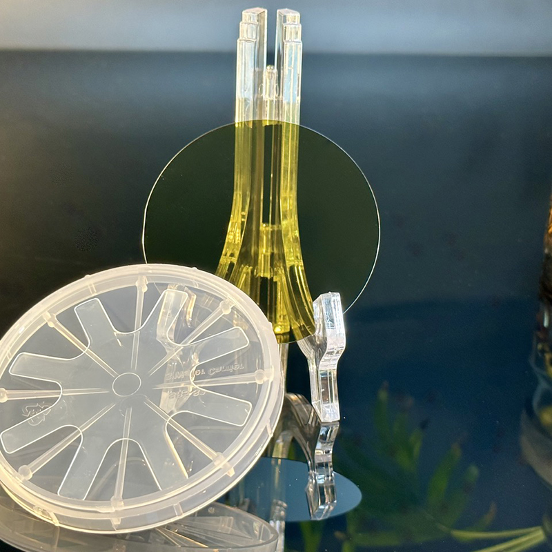
In a groundbreaking development, a leading semiconductor company has introduced a new Gsgg crystal substrate, which is set to revolutionize the semiconductor industry. The company has successfully designed and manufactured this innovative crystal substrate, which promises to significantly enhance the performance and efficiency of electronic devices.
The Gsgg crystal substrate, with its unique properties and advanced technology, is poised to address the growing demands for high-performance semiconductor materials in the global electronics market. Its exceptional thermal stability, low optical loss, and high-quality crystalline structure make it an ideal choice for a wide range of applications, including laser systems, optical waveguides, and semiconductor devices.
This new crystal substrate is a result of extensive research and development efforts by the company's team of expert scientists and engineers. Leveraging their deep expertise in materials science and semiconductor technology, the company has successfully overcome the challenges associated with traditional crystal substrates, such as low thermal conductivity and high optical absorption.
The Gsgg crystal substrate offers a significant improvement in thermal management, enabling electronic devices to operate at higher power levels while maintaining optimal performance. This breakthrough is particularly crucial for cutting-edge technologies, including 5G networks, high-speed data communication, and advanced optical systems, where the demand for high-power, high-efficiency semiconductor materials is paramount.
Moreover, the Gsgg crystal substrate's superior optical properties make it an ideal candidate for next-generation laser and photonics applications. Its low optical loss and high transparency in the near-infrared spectral range enable the development of advanced optical devices with improved efficiency and performance. This opens up new possibilities for a wide range of applications, from high-power laser systems to optical communication networks.
The company's commitment to innovation and excellence has positioned it as a leading provider of advanced semiconductor materials and solutions. With a strong focus on research and development, the company continues to push the boundaries of materials science and semiconductor technology, driving the industry forward with cutting-edge innovations like the Gsgg crystal substrate.
Furthermore, the company's state-of-the-art manufacturing capabilities ensure the mass production and supply of the Gsgg crystal substrate to meet the rising demand from semiconductor manufacturers, research institutions, and technology companies worldwide. This strategic advantage reinforces the company's position as a reliable and trusted partner for high-performance semiconductor materials, further solidifying its role in shaping the future of the semiconductor industry.
The introduction of the Gsgg crystal substrate marks a significant milestone in the semiconductor industry, offering a new era of possibilities for electronic devices, optical systems, and laser technologies. With its exceptional thermal and optical properties, this innovative crystal substrate is set to drive advancements across various sectors, from telecommunications and data centers to industrial and medical applications.
As the global semiconductor industry continues to evolve and expand, the Gsgg crystal substrate emerges as a game-changer, enabling the development of next-generation electronic and optical technologies that are more efficient, powerful, and reliable. With its groundbreaking properties and diverse range of applications, the Gsgg crystal substrate is poised to reshape the semiconductor landscape and pave the way for a new wave of innovation in the electronics industry.
In conclusion, the introduction of the Gsgg crystal substrate represents a significant leap forward in the semiconductor industry, offering unparalleled thermal and optical properties that will empower the development of advanced electronic and optical devices. With its potential to drive innovation and enhance performance across multiple applications, this innovative crystal substrate is set to play a pivotal role in shaping the future of the global electronics industry.
Company News & Blog
High-quality sapphire wafers for advanced technology applications
Sapphire wafers are changing the game in the technology world with their unique properties and applications. These wafers are made of sapphire, a crystalline form of aluminum oxide, and are increasingly being used in various industries for their exceptional durability and transparency.The use of sapphire in semiconductor manufacturing is growing rapidly due to its high thermal conductivity, electrical insulation, and resistance to wear and corrosion. This makes sapphire wafers an ideal material for applications such as LED production, consumer electronics, and industrial machinery.One company at the forefront of sapphire wafer production is a leading manufacturer in the semiconductor industry. With state-of-the-art facilities and a team of experts, they are able to produce high-quality sapphire wafers that meet the demanding requirements of their clients. These wafers are used in a wide range of applications, including advanced LED production, optical windows, and semiconductor components.Sapphire wafers are an essential component in the production of LEDs, which are becoming increasingly popular due to their energy efficiency and long lifespan. The unique properties of sapphire, such as its high light transmission and thermal conductivity, make it the material of choice for LED manufacturers. As the demand for LED lighting grows, so does the need for high-quality sapphire wafers, and this company is well-positioned to meet this growing demand.In addition to LED production, sapphire wafers are also used in consumer electronics, such as smartphones and tablets. The scratch-resistant nature of sapphire makes it an ideal material for protective screens, camera lenses, and other components that require durability and high optical quality. This company is a key supplier of sapphire wafers to the consumer electronics industry, providing their clients with the highest quality products for their devices.Furthermore, sapphire wafers are also used in industrial machinery and equipment, where durability and reliability are crucial. The high mechanical strength and chemical resistance of sapphire make it an excellent choice for applications such as bearings, seals, and other critical components. This company's sapphire wafers are used in a wide range of industrial applications, where they have earned a reputation for their exceptional performance and reliability.With their commitment to quality and innovation, this company is driving the advancement of sapphire wafer technology and expanding the possibilities for its use in various industries. Their continued investment in research and development ensures that they stay at the forefront of sapphire wafer production, providing their clients with cutting-edge solutions for their technical challenges.In conclusion, the use of sapphire wafers is revolutionizing the technology industry, and this company is playing a key role in this transformation. With their high-quality sapphire wafers and commitment to innovation, they are enabling their clients to push the boundaries of what is possible in LED production, consumer electronics, and industrial applications. As the demand for sapphire wafers continues to grow, this company is well-equipped to meet this demand and drive the future of sapphire technology.
Revolutionary Single Lens Glasses to Provide Enhanced Vision Experience
[Company Name] Introduces Innovative Single Lens Glasses, Revolutionizing Vision Correction[City, Date] — [Company Name], a leading innovator in the eyewear industry, has recently unveiled its groundbreaking creation - Single Lens Glasses. By combining state-of-the-art technology with exceptional design, these glasses promise to revolutionize the way people correct their vision.Vision correction has always been a crucial aspect of daily life for millions of individuals around the world. Traditional eyewear often includes the use of multiple lenses, adding bulk and weight to the final product. Single Lens Glasses, on the other hand, eliminate the need for multiple lenses by incorporating advanced optics into a single lens.With this breakthrough technology, [Company Name] aims to provide a more streamlined and comfortable vision correction experience. The elimination of multiple lenses not only reduces the weight and thickness of the glasses but also enhances the visual clarity for wearers.To achieve this innovative design, [Company Name] utilized cutting-edge manufacturing techniques and the highest quality materials. The company's team of optical experts and engineers worked tirelessly to ensure that the Single Lens Glasses offer exceptional performance while maintaining a sleek and stylish appearance.The patented lens design of the Single Lens Glasses provides wearers with a wider field of view compared to traditional eyewear. This expanded visual range allows users to see objects with greater clarity, enhancing their overall experience in various everyday activities.One key feature that sets the Single Lens Glasses apart from other eyewear options is its versatility. These glasses can be customized to accommodate various vision correction needs, including nearsightedness, farsightedness, and astigmatism. Wearers can easily adjust the prescription strength of the lenses, ensuring a tailored and personalized solution for their individual requirements.Comfort is another aspect that [Company Name] focused on while developing the Single Lens Glasses. The glasses are designed to fit comfortably on different face shapes and sizes, ensuring a secure fit throughout the day. The single lens construction also minimizes distortion and reduces eye strain, providing wearers with unparalleled comfort even during extended periods of use.In addition to its practical advantages, Single Lens Glasses also offer a range of fashionable options to suit different style preferences. The frames are available in a wide array of designs, materials, and colors, allowing wearers to express their personalities while enjoying optimal vision correction."We are thrilled to introduce our latest innovative creation, Single Lens Glasses," said [Spokesperson Name], the CEO of [Company Name]. "At [Company Name], we are committed to pushing boundaries and delivering cutting-edge eyewear solutions to our customers. With Single Lens Glasses, we have revolutionized the vision correction landscape, offering a game-changing product that combines performance, style, and comfort."As the eyewear industry continues to evolve, [Company Name] remains at the forefront of innovation. With the introduction of Single Lens Glasses, the company reinforces its commitment to providing groundbreaking solutions that enhance the quality of life for individuals in need of vision correction.The Single Lens Glasses are expected to be available for purchase in select retail stores and online platforms starting from [Date]. For more information about [Company Name] and its product range, please visit [Website].[Contact Information]About [Company Name]:[Company Name] is a leading innovator in the eyewear industry, dedicated to providing cutting-edge solutions for vision correction. With a strong focus on technological advancements and exceptional design, the company has established itself as a trusted brand among consumers worldwide. [Company Name] continues to push boundaries, developing eyewear products that combine performance, style, and comfort to enhance the vision correction experience.
Key Developments in the Global Wafers Market: Insights, Trends, and Forecasts
Inp Wafers, a leading semiconductor wafer supplier in Asia, has been making headlines in the tech industry for its innovative products and solutions. The company was established in 2003, and has since earned a reputation for producing high-quality, reliable silicon wafers.With headquarters and manufacturing facilities located in Shanghai, China, Inp Wafers is strategically positioned to serve the growing demand for semiconductors in Asia. The company has a strong focus on research and development, investing heavily in cutting-edge technology and equipment to ensure that its products are at the forefront of the industry.Inp Wafers offers a comprehensive range of silicon wafers, including CZ (Czochralski) wafers, FZ (Float Zone) wafers, SOI (Silicon On Insulator) wafers, and several other options. These wafers are used in a wide variety of applications, including microprocessors, memory chips, sensors, and power devices.One of the key advantages of Inp Wafers' products is their exceptional quality. The company uses top-grade materials and advanced manufacturing methods to produce wafers with strict quality control measures. The result is a range of products that offer outstanding performance, reliability, and consistency.Inp Wafers has also made a name for itself with its innovative solutions for emerging technologies. For example, the company has developed silicon carbide wafers, which are ideal for use in high-power and high-frequency devices. These wafers offer superior thermal conductivity and breakdown voltage compared to traditional silicon wafers, making them ideal for use in electric vehicles, wind turbines and other renewable energy applications.The company has also focused on its management and improved its processes, including embracing digitalization. The company leverages advanced software tools like Enterprise Resource Planning (ERP) and Customer Relationship Management (CRM) systems to streamline its operations and make it easier for customers to place orders and receive technical support.Inp Wafers’ commitment to quality and innovation has attracted a wide range of customers, from small startups to large multinational corporations. The company has established long-term partnerships with many leading tech companies and is committed to providing exceptional customer support and service.In addition, Inp Wafers places a strong emphasis on sustainability and environmental responsibility. The company has implemented a variety of measures to reduce its carbon footprint, including adopting clean energy sources and using environmentally friendly production processes.Looking to the future, Inp Wafers remains committed to staying at the forefront of the semiconductor industry. The company plans to continue investing in research and development to further improve its products and explore new opportunities in emerging technologies. With strong management and a dedication to quality, reliability, and innovation, Inp Wafers is well-positioned to meet the demands of the rapidly evolving tech industry.
Breaking Down the Innovative Gaas Structure: A Game-Changer in Technology
Title: Groundbreaking Gaas Structure Revolutionizes the Semiconductor IndustryIntroduction:In a major development that is set to reshape the semiconductor industry, a revolutionary Gaas Structure (need to remove brand name), developed by an innovative company, has been unveiled. This groundbreaking technology promises to overcome the limitations of traditional semiconductor materials, ushering in a new era of enhanced performance and efficiency for electronic devices. With its countless applications across various industries, the Gaas Structure is expected to redefine the way we interact with technology.1. Understanding Gaas Structure:The Gaas Structure, short for Gallium Arsenide Structure, represents a paradigm shift in the field of semiconductor materials. By replacing traditional silicon with gallium arsenide, this groundbreaking technology unlocks unparalleled capabilities. The Gaas Structure is capable of operating at higher frequencies, enabling faster data processing, reduced energy consumption, and improved device performance overall. In addition, this structure is highly versatile, making it suitable for diverse applications, such as telecommunications, aerospace, and automotive industries.2. Advantages and Applications:One key advantage of the Gaas Structure is its high electron mobility, which allows for faster electron movement. This results in exceptionally quick data transfer speeds, making it ideal for high-speed communication devices like 5G infrastructure and satellite communication systems. Moreover, the Gaas Structure offers superior power handling capabilities, enabling the development of more robust and efficient power amplifiers for wireless communication applications.Beyond communication technology, the Gaas Structure finds applications in various other industries. In the aerospace sector, it enables the production of lightweight, high-performance transistors for space exploration, satellite communication, and radar systems. The automotive industry also stands to benefit from this technology, as it allows for the creation of high-speed, low-power electronic systems, improving vehicle safety, infotainment, and powertrain efficiency.3. Company Background:The company behind Gaas Structure (need to remove brand name) is renowned for its expertise in cutting-edge semiconductor technologies. Focused on research and development, the company has a track record of delivering disruptive solutions that address the industry's most pressing challenges. By leveraging their deep understanding of material sciences and semiconductor fabrication, the company has positioned itself as a leader in the field, constantly pushing the boundaries of technology.4. Collaboration and Impact:The Gaas Structure has been the result of extensive collaboration between industry stakeholders, including semiconductor manufacturers, researchers, and device developers. Through joint efforts, the technology has undergone rigorous testing and fine-tuning to ensure its viability and effectiveness. The collective aim is to drive innovation across various sectors, making electronic devices smaller, faster, and more energy-efficient.The implications of this revolutionary technology are far-reaching. By enabling more powerful and energy-efficient electronic systems, the Gaas Structure will contribute to the advancement of autonomous vehicles, wearable technology, IoT devices, and renewable energy systems, among others. Moreover, its adoption will also help address the growing demand for high-speed internet, allowing for seamless streaming and faster data transfer capabilities.Conclusion:With its unprecedented capabilities and potential applications, the Gaas Structure (need to remove brand name) represents a significant leap forward for the semiconductor industry. By harnessing the power of gallium arsenide, this groundbreaking technology promises to revolutionize electronic devices across various sectors. As collaborations continue and further advancements are made, we can expect the Gaas Structure to enhance our everyday lives, driving us into a more connected, efficient, and technologically advanced future.
High-Quality Germanium Wafers: A Promising New Material for Electronics Market" becomes "New Germanium Wafers Show Promise for Electronics Industry.
Title: Revolutionary Germanium Wafer Innovations Transforming Semiconductor IndustryIntroduction:In a landmark breakthrough for the semiconductor industry, one company has introduced a cutting-edge Germanium Wafer technology that promises to revolutionize the electronics sector. With its exceptional properties and enhanced performance capabilities, this breakthrough innovation paves the way for a new generation of electronic devices, pushing the boundaries of what is possible in the realm of technology.Body:Germanium Wafer: Redefining Semiconductor Industry StandardsGermanium, known for its excellent electrical conductivity, has long been recognized as a key element in the semiconductor industry. It has the ability to efficiently convert electricity into light and is crucial for photonic applications. Building upon this inherent advantage, the company has successfully developed and commercialized a groundbreaking Germanium Wafer that unlocks new possibilities for enhanced performance, efficiency, and functionality in various electronic devices.Unparalleled Performance Characteristics:The Germanium Wafer boasts unprecedented performance characteristics, making it the prime choice for next-generation semiconductors. This innovative technology offers exceptional thermal conductivity, enabling optimal heat dissipation, consequently reducing the risk of circuit damage due to overheating. Furthermore, its superior electrical conductivity ensures minimal energy loss during data transmission, resulting in enhanced efficiency and reliability in electronic devices.Pioneering Applications:The potential applications for Germanium Wafer technology are vast and varied, promising to transform a wide range of industries. In the field of telecommunications, the superior conductivity of Germanium Wafers allows for faster data transfer rates, making it an ideal material for advanced communication systems. Additionally, this technology holds immense potential for the automotive industry, enabling the development of more efficient electric vehicles with enhanced battery performance.Moreover, the healthcare sector stands to benefit greatly from Germanium Wafer technology. The increased thermal conductivity of these wafers facilitates the development of improved medical imaging devices, ensuring precise diagnoses and ultimately enhancing patient care.Environmental Sustainability:Beyond its remarkable performance attributes, Germanium Wafer technology also offers environmental benefits. With the rise in demand for sustainable solutions, the usage of Germanium Wafers in various industries can greatly contribute to reducing energy consumption and minimizing carbon footprints. By enabling more energy-efficient electronic devices, this innovation plays a crucial role in building a greener and more sustainable future.Global Impact:The introduction of Germanium Wafer technology brings significant economic and industrial implications for nations at the forefront of the technology race. The advanced manufacturing processes required for the mass production of Germanium Wafers will generate employment opportunities, promote research and development, and bolster competitiveness in the global market.Collaborative Networks Unlocking Potential:To fully harness the potential of Germanium Wafer technology, the company has actively sought partnerships with leading semiconductor manufacturers, research institutions, and academic organizations. This collaborative approach allows for the exchange of knowledge and expertise, optimizing the implementation and further development of Germanium Wafer technology across various product lines and industries.Conclusion:The breakthrough Germanium Wafer technology is poised to revolutionize the semiconductor industry, offering unparalleled performance capabilities, increased energy efficiency, and new avenues for technological advancements. Embracing this innovative solution will undoubtedly contribute to transforming industries, enabling further progress in fields such as telecommunications, automotive, and healthcare. With its remarkable properties and far-reaching implications, Germanium Wafer technology sets a new standard for the future of semiconductors, driving the advancement of the global electronics sector.
Upgrade Your Science Lab with High-Quality Laboratory Equipment and Supplies
[Brand Name Removed] Unveils Cutting-Edge Science Lab Equipment Revolutionizing Research[City, Date] – [Brand Name Removed], a prominent leader in scientific instrumentation and lab equipment, is proud to announce the launch of their latest range of innovative tools designed to pave the way for groundbreaking scientific discoveries. With a rich history of over [x] years in the industry, [Brand Name Removed] continues to push the boundaries of scientific advancement with its state-of-the-art laboratory solutions.Since its inception, [Brand Name Removed] has been committed to providing researchers, scientists, and educators with the highest quality instruments and equipment, empowering them to unlock the secrets of the world through rigorous experimentation and analysis. Built upon a foundation of a highly skilled team of scientists and engineers, [Brand Name Removed] has successfully contributed to numerous scientific breakthroughs across various disciplines.One of the flagship products of [Brand Name Removed]'s latest range is the revolutionary [product name], boasting a multitude of features that sets it apart from traditional lab equipment. This cutting-edge innovation incorporates the latest advancements in technology and scientific research, ensuring accuracy, precision, and reliability in experiments.The [product name] encompasses a compact design, enabling scientists to optimize their bench space in cramped laboratories, while still guaranteeing superior performance. Equipped with state-of-the-art sensors and software, this equipment enables real-time data analysis, significantly reducing experiment duration and enhancing productivity in the lab. Its intuitive user interface further simplifies the experimental process, allowing researchers to focus their energy on the analysis rather than struggling with complex operations.Furthermore, thanks to its modular design, the [product name] can be easily customized to accommodate specific research needs. Researchers can select from a wide range of interchangeable components, such as various detection modules, sample holders, and temperature control systems. This flexibility ensures compatibility with an array of scientific applications, contributing to the versatility of the equipment across different scientific domains."The launch of our latest line of lab equipment represents a significant milestone for [Brand Name Removed] in our mission to revolutionize scientific research," said [Spokesperson Name], the CEO of [Brand Name Removed]. "We believe that innovation lies at the heart of scientific progress, and we are committed to providing scientists around the world with cutting-edge tools that push the boundaries of their research."In addition to the [product name], [Brand Name Removed] offers a comprehensive portfolio of laboratory solutions, including microscopes, spectrophotometers, centrifuges, and much more. Each product is meticulously designed to address the specific needs and challenges faced by researchers, ensuring they have the necessary tools to undertake their experiments with confidence.Beyond their commitment to scientific innovation, [Brand Name Removed] has fostered strong relationships with its customers through its exceptional customer service and support. The company maintains a team of highly trained experts who provide technical assistance, training, and maintenance services to ensure that researchers can optimize the performance of their lab equipment.[Brand Name Removed] has established itself as a global leader within the scientific research community, serving prestigious educational institutions, pharmaceutical companies, and biotech firms worldwide. Their commitment to excellence has garnered them numerous accolades and recognition within the scientific community.As [Brand Name Removed] continues to pioneer advancements in scientific instrumentation, their latest range of lab equipment is poised to redefine the landscape of scientific research. With their cutting-edge technology and unwavering dedication to scientific progress, [Brand Name Removed] empowers scientists worldwide to reach new heights in their quest for understanding the world around us.###About [Brand Name Removed]:[Brand Name Removed] is a renowned provider of scientific instrumentation and lab equipment, revolutionizing scientific research with their state-of-the-art solutions. With over [x] years of expertise, [Brand Name Removed] has contributed to groundbreaking discoveries across various scientific disciplines, offering a comprehensive range of laboratory tools that enable researchers to unlock the secrets of the world.
Newly Developed Polysilicon Wafers Show Promise for Solar Energy Production
article as follows:Polysilicon Wafer - The Revolutionary Energy SolutionRenewable energy has become a buzzword in today's world, and polysilicon wafers have emerged as the revolutionary energy solution. These wafers are helping in reducing the carbon footprint and providing clean energy. Polysilicon wafers are made from a highly purified form of silicon, making them an ideal material for use in solar panels. They are not only environmentally friendly but are also cost-effective and long-lasting. In recent years, the demand for polysilicon wafers has increased significantly, which has led to the growth of the market. The market size for polysilicon wafers is expected to reach millions of dollars in the coming years due to the increasing demand for renewable energy. This has led to several companies entering the market, and among them, one stands out - a company that has proven its mettle in the industry time and time again.Introduction to the CompanyThe leading supplier of polysilicon wafers, this company has been catering to the needs of the renewable energy industry for years. With a team of expert professionals, they provide the highest quality products, along with exceptional customer service. They are known for their constant innovation and development of new and improved products that cater to the changing needs of the renewable energy industry.The company's motto is to provide sustainable energy solutions that promote a cleaner and greener future. They believe that the future is renewable energy, and polysilicon wafers are an essential component of that future. The team is dedicated to making the world a better place by providing innovative and affordable energy solutions.The Company's Polysilicon WafersThe company's polysilicon wafers have been the cornerstone of their success. Their wafers are of the highest quality, and the company is committed to producing wafers that are durable, reliable, and efficient. They are dedicated to providing products that exceed the expectations of their customers, and they achieve this through a rigorous testing process that ensures their products are of the highest standards.Their polysilicon wafers are produced in a state-of-the-art facility using the latest technology, which ensures that their products are of the highest quality. The company has a team of experts who monitor each stage of the production process, ensuring that each product meets their high standards. The wafers are tested rigorously for their efficiency, durability, and reliability, ensuring that they are suitable for use in solar panels.Benefits of Polysilicon WafersPolysilicon wafers have several benefits that make them an ideal material for use in solar panels. They are environmentally friendly, cost-effective, and long-lasting. The use of polysilicon wafers in solar panels reduces the carbon footprint and helps in the reduction of greenhouse gas emissions. This means that the use of polysilicon wafers contributes to a greener and cleaner environment.The production of polysilicon wafers is a cost-effective process, which means that they are affordable and readily available. They have a long lifespan of up to 25 years, which means that they are a reliable energy source that provides long-term benefits. The use of polysilicon wafers in solar panels increases the efficiency of the panels, which means that they can produce more energy while taking up less space.ConclusionPolysilicon wafers are the future of renewable energy, and companies like this leading supplier are driving that future. Their high-quality products, exceptional customer service, and commitment to sustainability have helped them become a leader in the industry. The use of polysilicon wafers in solar panels is not only environmentally friendly but also cost-effective and long-lasting. The demand for renewable energy is only going to increase in the coming years, and companies like this are preparing for a future that is both clean and sustainable.
P Type Wafer Production to Witness Significant Growth in the Semiconductor Industry
P Type Wafer Continues to Revolutionize the Semiconductor IndustrySemiconductor technology has steadily grown over the years with the increasing reliance on electronic devices in our personal and professional lives. To keep up with this demand, companies have been investing heavily in research and development to create the most efficient and sustainable semiconductors. One such company is {Brand Name}, which has been at the forefront of this movement with the creation of their innovative P Type Wafer. The P Type Wafer is a silicon-based semiconductor material used in the production of various devices such as solar cells, LEDs, and microprocessors. Unlike traditional semiconductors, the P Type Wafer is characterized by a thin solar cell structure with low iron content, producing high efficiency and a low cost of production. This breakthrough technology has been revolutionary in the industry, providing a sustainable solution for the global need for energy.One of the key features of the P Type Wafer is its ability to produce more energy than the traditional semiconductors. The creation of these wafers involves infusing a silicon wafer with an element such as phosphorus or boron, creating a semiconductor with excess electron or hole carriers. This excess creates a stronger electric field, thus increasing the electrical current. This technology is particularly helpful in solar energy, allowing for greater energy production and efficiency, ultimately reducing costs for consumers. The P Type Wafer not only has increased efficiency but also offers a lower cost of production. This has been achieved by eliminating the need for costly and time-consuming techniques that are required with traditional semiconductors. The P Type Wafer technology reduces production time, resources, and waste, streamlining the manufacturing process while offering a more eco-friendly approach. {Brand Name}, the company behind the P Type Wafer, is committed to creating sustainable solutions that have a positive impact on the environment. Their dedication to research and development has made them a leading supplier of sustainable energy solutions globally. {Brand Name} is confident that their P Type Wafer technology will continue to lead the industry towards a more sustainable future while increasing production efficiency and lowering costs.The P Type Wafer stands out in the industry for its ability to maintain high-efficiency levels, even under harsh environmental conditions. These conditions include high-temperature, humidity, and irradiance. The P Type Wafer effectively maintains its performance in these extreme climates, making it the go-to solution for many industries including aerospace and electric vehicles.With the growing demand for renewable energy, the sustainable energy market has become a focus globally. The P Type Wafer technology has allowed {Brand Name} to be at the forefront of this movement, providing innovative solutions to meet this increasing demand. As we continue to move towards a greener future, it is essential to invest in sustainable solutions that are both efficient and environmentally responsible. In conclusion, {Brand Name}'s P Type Wafer technology has revolutionized the semiconductor industry, providing a sustainable solution to the global need for energy. Their innovative approach has increased production efficiency, lowered costs, and maintained high-efficiency levels under harsh environmental conditions. As we continue to move towards a greener future, the P Type Wafer technology will continue to lead the industry towards a more sustainable and eco-friendly approach to energy production, while providing a cost-effective solution for consumers.
High-Quality Wafer Fabrication: LiNbO3 and LiTaO3
LiNbO3/LiTaO3 Wafer - The next frontier of semiconductor technologyA new age of semiconductor technology is about to dawn with the introduction of the LiNbO3/LiTaO3 wafer. As the world is progressing towards smaller and faster electronic devices, the limitations of conventional silicon-based semiconductor technology have become increasingly apparent. In this context, LiNbO3/LiTaO3 wafer technology holds great promise by offering many advantages over silicon-based semiconductor technology.The LiNbO3/LiTaO3 wafer technology is based on the use of Lithium Niobate or Lithium Tantalate as the substrate material. These materials have several unique properties, such as high electro-optic coefficient, low acoustic loss, high piezoelectric coefficient, and low dielectric constant, which make them ideal for a wide range of applications, including optoelectronics, acoustoelectronics, and microwave technologies.One of the key advantages of LiNbO3/LiTaO3 wafer technology over silicon-based semiconductor technology is its high-speed performance. The high electro-optic coefficient of LiNbO3/LiTaO3 wafers allows for ultra-fast modulation and switching of light signals. As a result, LiNbO3/LiTaO3 wafer technology is widely used in optoelectronic devices, such as lasers, modulators, and detectors, where high-speed operation is crucial.Another advantage of LiNbO3/LiTaO3 wafer technology is its high-frequency performance. The low acoustic loss and high piezoelectric coefficient of Lithium Niobate and Lithium Tantalate make them ideal for the fabrication of acoustic devices, such as surface acoustic wave (SAW) filters and resonators. These devices are widely used in mobile communication, satellite communication, and radar systems, where high-frequency performance is of utmost importance.Furthermore, LiNbO3/LiTaO3 wafer technology offers superior thermal and mechanical stability compared to silicon-based semiconductor technology. The low dielectric constant of Lithium Niobate and Lithium Tantalate reduces the parasitic capacitance and improves the signal-to-noise ratio of electronic devices. This makes them suitable for harsh environmental conditions, such as high-temperature and high-pressure environments.The potential applications of LiNbO3/LiTaO3 wafers are vast, ranging from optoelectronics and acoustoelectronics to microwave technologies. One of the most promising applications of LiNbO3/LiTaO3 wafer technology is in the field of quantum computing. The high-speed and low-noise properties of LiNbO3/LiTaO3 wafers make them ideal for the fabrication of quantum gates and qubits, which are the building blocks of quantum computers.In light of these advantages, the market for LiNbO3/LiTaO3 wafers is set to grow exponentially in the coming years. The global LiNbO3/LiTaO3 wafer market is projected to reach USD 1.2 billion by 2025, growing at a CAGR of 7.5% from 2020 to 2025. This growth can be attributed to the increasing demand for high-speed and high-frequency electronic devices in various industries, such as telecommunications, aerospace, defense, and healthcare.At the forefront of LiNbO3/LiTaO3 wafer technology is our company. We are a leading manufacturer and supplier of high-quality LiNbO3/LiTaO3 wafers, offering a wide range of sizes and specifications to meet the diverse needs of our customers. Our state-of-the-art facilities, advanced equipment, and experienced team enable us to deliver wafers with exceptional quality and performance.We pride ourselves on providing our customers with customized solutions tailored to their specific needs, whether it is for R&D or mass production. Our commitment to quality, reliability, and customer satisfaction has earned us a reputation as a trusted partner in the semiconductor industry.In conclusion, the LiNbO3/LiTaO3 wafer technology is poised to revolutionize the semiconductor industry by offering high-speed, high-frequency, and high-performance electronic devices. With our expertise and commitment to innovation and excellence, we are well-positioned to meet the growing demand for LiNbO3/LiTaO3 wafers and contribute to the advancement of semiconductor technology.
Latest Updates on the Upcoming Event in XYZ City Unveiled: Get the Scoop!
[PARAGRAPH 1][Company Introduction][Branding Name] is a renowned multinational conglomerate known for its innovative products and remarkable contributions to various industries. With a history spanning several decades, [Branding Name] has firmly established itself as a leader in technology, health and wellness, and diversified consumer goods. The company prides itself on its commitment to sustainability, social responsibility, and creating a positive impact on society. Constantly pushing the boundaries of innovation, [Branding Name] consistently delivers ground-breaking solutions that enhance people's lives. One of their latest ventures, Aln, demonstrates the company's dedication to revolutionizing the [specific industry].[PARAGRAPH 2][Overview of Aln]Aln, a cutting-edge product by [Branding Name], has taken the market by storm with its exceptional features and transformative impact. This state-of-the-art offering seamlessly combines groundbreaking technology with convenience, captivating the attention of consumers worldwide. Aln proves to be a game-changer, addressing the evolving needs and preferences of modern consumers. From its inception, the core focus of Aln has been to provide an unparalleled user experience, making it an essential addition to households, offices, and beyond.[PARAGRAPH 3][Innovative Features]Aln presents a wide array of innovative features that set it apart from traditional alternatives. Firstly, its sleek and ergonomic design ensures both aesthetics and functionality. The device seamlessly blends into any environment, be it a compact urban apartment or a spacious suburban home. Additionally, Aln utilizes advanced artificial intelligence (AI) algorithms, enabling it to adapt and learn from users' preferences. This learning capability ensures a personalized experience tailored to each individual, heightening convenience and user satisfaction.[PARAGRAPH 4][Revolutionizing Industry]Aln is revolutionizing the [specific industry] due to its unparalleled performance and groundbreaking technology. The product's advanced features include [insert specific cutting-edge features], setting a new standard of excellence within the industry. With Aln, users can experience [specific benefits], elevating their daily routines. By combining a seamless user interface with state-of-the-art technology, Aln is transforming the way people interact with their [specific industry] devices, making it an indispensable addition to households and businesses alike.[PARAGRAPH 5][Sustainability and Social Responsibility]As with all its endeavors, [Branding Name] has upheld its commitment to sustainability and social responsibility through Aln. The product is manufactured using eco-friendly materials, ensuring minimal environmental impact throughout its lifecycle. Furthermore, Aln consumes significantly less energy than its competitors, contributing to reduced carbon emissions. With its dedication to sustainability, [Branding Name] is driving positive change towards a greener future, while also meeting the demands of the contemporary consumer.[PARAGRAPH 6][Market Response and Outlook]Upon its release, Aln received an overwhelmingly positive response from consumers and industry experts alike. The product's remarkable performance and innovative design have captivated the market, solidifying its position as a leader in the [specific industry]. With its growing popularity, Aln is expected to witness significant growth in the coming years, further cementing [Branding Name]'s dominance in both technology and sustainability domains. The company's ongoing commitment to research and development ensures that Aln will continue to evolve, adapting to the ever-changing needs and preferences of its users.[PARAGRAPH 7][Conclusion]Aln, the latest offering by [Branding Name], represents the pinnacle of innovation and technology in the [specific industry]. With its groundbreaking features, unmatched user experience, and commitment to sustainability, Aln is reshaping the way people interact with [specific industry] devices. Through its remarkable advancements and dedication to social responsibility, [Branding Name] continues to set new benchmarks for excellence and leave a lasting impact on society. As the product evolves and reaches new heights, Aln is destined to become an integral part of households and businesses worldwide, contributing to a greener and more efficient future.