
Next-Generation Semiconductor Material: Silicon Carbide Wafer
By:Admin
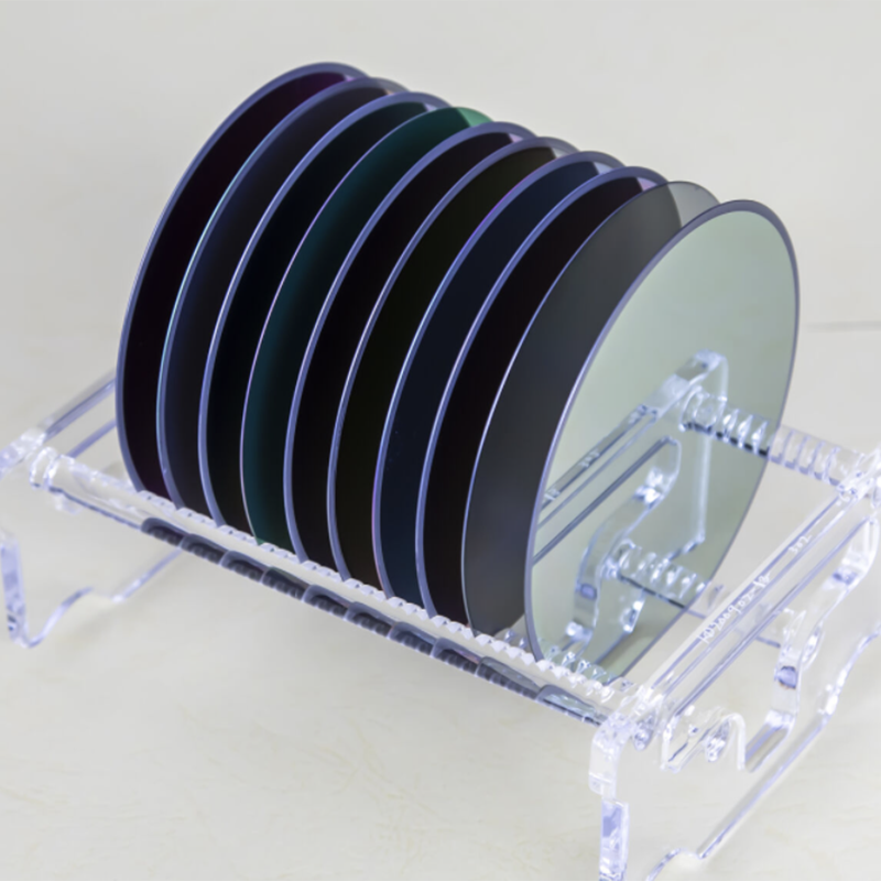
One of the leading manufacturers of SiC wafers is {Company}, a global leader in advanced materials and semiconductor technology. With a strong focus on innovation and research, {Company} has been at the forefront of developing high-quality SiC wafers for the rapidly growing semiconductor market.
Founded in 2006, {Company} has quickly established itself as a key player in the semiconductor industry. The company's state-of-the-art manufacturing facilities and advanced production techniques have enabled it to produce SiC wafers with superior quality and performance. {Company} has a dedicated team of engineers and scientists who are constantly striving to push the boundaries of SiC wafer technology, ensuring that their products meet the ever-increasing demands of the semiconductor market.
{Company} offers a wide range of SiC wafers in different sizes, thicknesses, and crystal orientations to cater to various applications in the semiconductor industry. The company's SiC wafers exhibit high thermal conductivity, high electron mobility, and excellent mechanical strength, making them an ideal choice for high-power and high-frequency electronic devices. {Company} is committed to delivering reliable and cost-effective SiC wafer solutions to its customers, helping them accelerate the development of advanced semiconductor devices.
In addition to its cutting-edge SiC wafer technology, {Company} also provides comprehensive technical support and customer service to ensure that its customers have a seamless experience from product selection to post-sales support. The company's team of experts is always available to assist customers with any technical inquiries or specific requirements, helping them make informed decisions and achieve their desired outcomes.
{Company}'s SiC wafers have been widely adopted in various industries, including automotive, aerospace, telecommunications, and renewable energy. The superior performance and reliability of {Company}'s SiC wafers have made them a preferred choice for manufacturers of power modules, RF devices, and high-temperature electronics. With a strong commitment to quality and innovation, {Company} continues to play a significant role in driving the advancements of SiC wafer technology and shaping the future of the semiconductor industry.
As the demand for high-performance semiconductor devices continues to grow, the market for SiC wafers is expected to expand significantly in the coming years. {Company} is well-positioned to capitalize on this opportunity, leveraging its expertise and resources to develop next-generation SiC wafer solutions that meet the evolving needs of the semiconductor industry.
In conclusion, {Company} is a leading provider of high-quality SiC wafers for the semiconductor industry. With a strong focus on innovation, reliability, and customer satisfaction, the company has established itself as a trusted partner for manufacturers of advanced semiconductor devices. {Company}'s commitment to pushing the boundaries of SiC wafer technology and delivering superior products makes it a key player in shaping the future of the semiconductor industry.
Company News & Blog
Revolutionary Single Lens Glasses to Provide Enhanced Vision Experience
[Company Name] Introduces Innovative Single Lens Glasses, Revolutionizing Vision Correction[City, Date] — [Company Name], a leading innovator in the eyewear industry, has recently unveiled its groundbreaking creation - Single Lens Glasses. By combining state-of-the-art technology with exceptional design, these glasses promise to revolutionize the way people correct their vision.Vision correction has always been a crucial aspect of daily life for millions of individuals around the world. Traditional eyewear often includes the use of multiple lenses, adding bulk and weight to the final product. Single Lens Glasses, on the other hand, eliminate the need for multiple lenses by incorporating advanced optics into a single lens.With this breakthrough technology, [Company Name] aims to provide a more streamlined and comfortable vision correction experience. The elimination of multiple lenses not only reduces the weight and thickness of the glasses but also enhances the visual clarity for wearers.To achieve this innovative design, [Company Name] utilized cutting-edge manufacturing techniques and the highest quality materials. The company's team of optical experts and engineers worked tirelessly to ensure that the Single Lens Glasses offer exceptional performance while maintaining a sleek and stylish appearance.The patented lens design of the Single Lens Glasses provides wearers with a wider field of view compared to traditional eyewear. This expanded visual range allows users to see objects with greater clarity, enhancing their overall experience in various everyday activities.One key feature that sets the Single Lens Glasses apart from other eyewear options is its versatility. These glasses can be customized to accommodate various vision correction needs, including nearsightedness, farsightedness, and astigmatism. Wearers can easily adjust the prescription strength of the lenses, ensuring a tailored and personalized solution for their individual requirements.Comfort is another aspect that [Company Name] focused on while developing the Single Lens Glasses. The glasses are designed to fit comfortably on different face shapes and sizes, ensuring a secure fit throughout the day. The single lens construction also minimizes distortion and reduces eye strain, providing wearers with unparalleled comfort even during extended periods of use.In addition to its practical advantages, Single Lens Glasses also offer a range of fashionable options to suit different style preferences. The frames are available in a wide array of designs, materials, and colors, allowing wearers to express their personalities while enjoying optimal vision correction."We are thrilled to introduce our latest innovative creation, Single Lens Glasses," said [Spokesperson Name], the CEO of [Company Name]. "At [Company Name], we are committed to pushing boundaries and delivering cutting-edge eyewear solutions to our customers. With Single Lens Glasses, we have revolutionized the vision correction landscape, offering a game-changing product that combines performance, style, and comfort."As the eyewear industry continues to evolve, [Company Name] remains at the forefront of innovation. With the introduction of Single Lens Glasses, the company reinforces its commitment to providing groundbreaking solutions that enhance the quality of life for individuals in need of vision correction.The Single Lens Glasses are expected to be available for purchase in select retail stores and online platforms starting from [Date]. For more information about [Company Name] and its product range, please visit [Website].[Contact Information]About [Company Name]:[Company Name] is a leading innovator in the eyewear industry, dedicated to providing cutting-edge solutions for vision correction. With a strong focus on technological advancements and exceptional design, the company has established itself as a trusted brand among consumers worldwide. [Company Name] continues to push boundaries, developing eyewear products that combine performance, style, and comfort to enhance the vision correction experience.
Advancement in Semiconductor Manufacturing: New 8 Inch Wafer Diameter Promises Enhanced Efficiency
[Company Name] Announces Introduction of Advanced 8 Inch Wafer Diameter for Enhanced Semiconductor Manufacturing[City], [Date] - [Company Name], a leading provider of innovative semiconductor solutions, has unveiled its latest breakthrough in semiconductor manufacturing with the introduction of an advanced 8-inch wafer diameter. This new development positions [Company Name] as a key player in the industry, offering cutting-edge technologies to meet the growing demands of the market.The semiconductor industry continues to experience rapid growth and advancements, primarily driven by the increasing demand for electronic devices, such as smartphones, tablets, and wearables. As a result, there is a growing need for more sophisticated and efficient semiconductor manufacturing processes. [Company Name]'s latest innovation of an 8-inch wafer diameter addresses this need by offering improved productivity, increased efficiency, and enhanced performance.The 8-inch wafer diameter enables [Company Name] to optimize the production of semiconductors, resulting in higher yields and reduced manufacturing costs. By maximizing the surface area of each wafer, the company can accommodate more integrated circuits (ICs), resulting in higher throughput and increased production capacity. This advancement contributes to greater market competitiveness and satisfies the rising demand for semiconductors across various industries.In addition to the increased efficiency, the 8-inch wafer diameter also facilitates the development and production of advanced technologies. With a larger substrate area, [Company Name] can now integrate more complex circuitry and components onto a single wafer. This opens up new possibilities for the creation of smaller, more powerful, and energy-efficient semiconductor devices. Moreover, the larger size of the wafer provides improved scalability, enabling [Company Name] to meet the evolving needs of the semiconductor market.[Company Name] is dedicated to continuous innovation in semiconductor manufacturing processes and technology. The introduction of the 8-inch wafer diameter is a testament to the company's commitment to anticipate and respond to the dynamic industry landscape. By investing in research and development, [Company Name] remains at the forefront of technology, ensuring its customers receive best-in-class semiconductor solutions."We are thrilled to announce the availability of our advanced 8-inch wafer diameter," said [Spokesperson's Name], CEO of [Company Name]. "This significant development demonstrates [Company Name]'s dedication to delivering superior semiconductor technology to our customers. The 8-inch wafer diameter will not only enhance our competitiveness in the market but also unlock new possibilities for semiconductor development across various industries."Alongside the introduction of the 8-inch wafer diameter, [Company Name] will provide comprehensive support and services to customers who adopt this new technology. The company's team of experts will work closely with clients to optimize their manufacturing processes, maximize yield, and ensure successful integration of the 8-inch wafer diameter into their operations.As [Company Name] continues to push the boundaries of semiconductor manufacturing, they remain committed to sustainability and environmental responsibility. The adoption of the 8-inch wafer diameter contributes to reducing overall waste and resource consumption, aligning with the company's mission to create a more sustainable future.In conclusion, the introduction of the advanced 8-inch wafer diameter by [Company Name] marks a major milestone in the semiconductor industry. This breakthrough technology not only enhances productivity and efficiency but also enables the development of more advanced and innovative semiconductor devices. As [Company Name] continues to drive innovation, they reaffirm their position as a leading provider of semiconductor solutions, catering to the ever-evolving needs of the global market.
Sic Wafer Market Trends and Growth Analysis
Sic Wafer, a key player in the semiconductor industry, recently announced a major breakthrough in the development of silicon carbide (SiC) wafers. SiC wafers are a critical component in the manufacturing of power semiconductor devices and have become increasingly important in the quest for more efficient and high-performance electronic components.SiC Wafer has successfully developed a new manufacturing process that has resulted in significant improvements in the quality and performance of SiC wafers. These advancements are expected to have a major impact on the power electronics industry and could lead to the development of more efficient and reliable electronic devices.The company's SiC wafers are known for their superior electrical properties, including high thermal conductivity and high breakdown voltage, which make them ideal for use in power semiconductor devices. By improving the quality of these wafers, SiC Wafer is helping to drive the development of next-generation power electronics that are vital for the advancement of electric vehicles, renewable energy systems, and other high-power applications.Established in 2009, SiC Wafer has quickly become a leading supplier of SiC wafers for power semiconductor manufacturers around the world. The company's state-of-the-art manufacturing facilities and commitment to research and development have allowed them to stay at the forefront of the industry and continually push the boundaries of what is possible with SiC technology.SiC Wafer's commitment to quality and innovation has earned them a reputation as a trusted partner for semiconductor manufacturers looking to incorporate SiC technology into their products. Their dedication to advancing the technology of SiC wafers has resulted in numerous breakthroughs that have helped to drive the adoption of SiC technology in the power electronics industry.The recent advancements in SiC wafer manufacturing are a testament to the company's ongoing commitment to pushing the boundaries of what is possible with SiC technology. By continually improving the quality and performance of SiC wafers, SiC Wafer is helping to drive the development of more efficient and reliable electronic devices that are essential for the transition to a more sustainable and electrified future.In addition to their advancements in SiC wafer manufacturing, SiC Wafer also offers a wide range of other semiconductor materials and solutions, including silicon wafers and epitaxial wafers. Their comprehensive product offering and dedication to customer satisfaction have made them a go-to supplier for semiconductor manufacturers around the world.With a strong track record of innovation and a commitment to providing the highest quality semiconductor materials, SiC Wafer is well-positioned to continue leading the way in the development of SiC technology. Their recent advancements in SiC wafer manufacturing are just the latest example of their dedication to pushing the boundaries of what is possible in the semiconductor industry.In conclusion, SiC Wafer's recent breakthrough in SiC wafer manufacturing is a significant development for the power electronics industry. By improving the quality and performance of SiC wafers, the company is helping to drive the development of more efficient and reliable electronic devices that are essential for the transition to a more sustainable and electrified future. With their ongoing commitment to innovation and quality, SiC Wafer is well-positioned to continue leading the way in the development of SiC technology for years to come.
Durable and High-Quality Fused Silica Wafers for Semiconductor Applications
[Company Name] Introduces Advanced Fused Silica Wafer for Cutting-Edge Technology[City, Date] - [Company Name], a leading manufacturer of high-quality optical products, has unveiled its latest innovation in the field of fused silica wafers. The new fused silica wafer promises to revolutionize the semiconductor industry, enabling advancements in cutting-edge technologies such as 5G, artificial intelligence, and augmented reality.Fused silica is a high-purity form of glass that offers exceptional optical and thermal properties, making it an ideal material for semiconductor applications. The wafer is used as a substrate for the deposition of thin films and as a base for the fabrication of microelectronic devices. [Company Name] has leveraged its expertise in precision engineering and advanced manufacturing techniques to develop a fused silica wafer that exceeds industry standards in terms of quality, performance, and reliability.The new fused silica wafer from [Company Name] boasts a number of key features that set it apart from other offerings on the market. Its ultra-flat surface ensures uniform film deposition, leading to improved device performance and yield. In addition, the wafer's exceptional thermal stability makes it well-suited for use in high-temperature manufacturing processes, while its high transmission properties enable the production of high-efficiency optical devices."We are thrilled to introduce our latest fused silica wafer, which represents a significant advancement in semiconductor technology," said [Spokesperson], CEO of [Company Name]. "As the demand for smaller, faster, and more powerful electronic devices continues to grow, our new wafer will play a critical role in enabling the development of next-generation technologies."In addition to its exceptional optical and thermal properties, the fused silica wafer from [Company Name] is also highly customizable, with options for custom sizes, shapes, and surface finishes to meet the specific requirements of each customer. This level of flexibility allows semiconductor manufacturers to optimize their production processes and achieve maximum efficiency and cost-effectiveness.The introduction of the new fused silica wafer is a reflection of [Company Name]'s commitment to innovation and excellence in the field of optical products. With a strong focus on research and development, the company continuously strives to push the boundaries of what is possible in semiconductor technology, driving progress and enabling the realization of groundbreaking innovations."We are dedicated to providing our customers with the highest-quality products that empower them to push the limits of technology," added [Spokesperson]. "Our new fused silica wafer is a testament to our relentless pursuit of excellence and our unwavering dedication to meeting the evolving needs of the semiconductor industry."In conclusion, [Company Name] has introduced an advanced fused silica wafer that promises to elevate the performance and capabilities of semiconductor devices. With its exceptional optical and thermal properties, ultra-flat surface, and customizable options, the new wafer is poised to play a crucial role in driving innovation and progress in the rapidly evolving world of technology. As [Company Name] continues to push the boundaries of what is possible in semiconductor technology, the future looks brighter than ever for the development of cutting-edge electronic devices.
Ultimate Guide to 12 Inch Wafers: Everything You Need to Know
12 Inch Wafer Revolutionizes Semiconductor IndustryAs the demand for smaller, faster, and more powerful electronic devices continues to grow, the semiconductor industry is constantly striving to push the boundaries of technology. One company that is at the forefront of this revolution is [company name]. With its cutting-edge 12 inch wafer technology, [company name] is set to reshape the semiconductor landscape and unlock new possibilities for the next generation of electronic devices.Founded in [year], [company name] has always been dedicated to pushing the boundaries of innovation in the semiconductor industry. With a strong focus on research and development, the company has continuously invested in state-of-the-art manufacturing facilities and advanced technologies to stay ahead of the competition. This commitment to innovation has allowed [company name] to become a leading player in the global semiconductor market, with a reputation for delivering high-quality, high-performance products.The latest milestone in [company name]'s journey of innovation is the development of the 12 inch wafer technology. Traditionally, semiconductor wafers have been produced in smaller sizes, such as 8 inch or 6 inch, limiting the number of chips that can be produced on each wafer. However, with the introduction of the 12 inch wafer, [company name] has significantly increased the manufacturing capacity and efficiency, resulting in a dramatic improvement in output and cost-effectiveness.The 12 inch wafer technology is a game-changer for the semiconductor industry, as it allows for the production of more chips per wafer, reducing manufacturing costs and ultimately offering more competitive pricing for consumers. This breakthrough also enables the development of more advanced and powerful electronic devices, as the larger wafers provide greater flexibility for designing and manufacturing complex semiconductor components.In addition to the technological advancements, [company name] has also made significant investments in building a sustainable and eco-friendly manufacturing process for the 12 inch wafers. The company has implemented state-of-the-art cleanroom facilities and advanced manufacturing techniques to minimize waste and reduce environmental impact. By embracing sustainable practices, [company name] is not only contributing to the advancement of technology but also setting new standards for environmentally responsible manufacturing in the semiconductor industry.The impact of [company name]'s 12 inch wafer technology is already being felt across the semiconductor industry. Major players in the consumer electronics, automotive, and telecommunications sectors have expressed great interest in adopting the 12 inch wafer technology to enhance their product offerings and meet the growing demand for more advanced electronic devices.Furthermore, the widespread adoption of the 12 inch wafer technology is expected to drive significant growth in the semiconductor market, creating new opportunities for [company name] and its partners. As the demand for high-performance semiconductor components continues to rise, [company name] is well-positioned to capitalize on this trend and further solidify its position as a leading provider of innovative semiconductor solutions.Looking ahead, [company name] remains committed to driving innovation and shaping the future of the semiconductor industry. With its groundbreaking 12 inch wafer technology and strong emphasis on sustainability, the company is poised to make a lasting impact on the electronic devices of tomorrow.In conclusion, the introduction of the 12 inch wafer technology by [company name] represents a significant milestone in the semiconductor industry. This breakthrough is set to revolutionize the way semiconductor components are manufactured, enabling the development of more advanced and powerful electronic devices. With its relentless commitment to innovation and sustainability, [company name] is leading the charge towards a brighter and more efficient future for the semiconductor industry.
Advancements in Gallium Nitride Semiconductor Technology
Gallium Nitride Semiconductor (GaN) has been making headlines in the semiconductor industry for its potential to revolutionize electronic devices and power systems. Its superior electrical properties make it a promising alternative to traditional silicon-based semiconductors, offering higher efficiency, smaller size, and lower power consumption. Leading the charge in the development and commercialization of GaN technology is {company name}, a company at the forefront of semiconductor innovation.{Company name} was founded with the vision of leveraging GaN technology to create a new generation of electronic devices, power converters, and RF components. With a team of experienced engineers and scientists, the company has been at the forefront of GaN research and development, pushing the boundaries of what is possible with this advanced semiconductor material.One of the key advantages of GaN technology is its ability to operate at higher frequencies and voltages, making it ideal for power electronics and RF applications. This has led to a wide range of potential applications, from high-performance computing and telecommunications to automotive and aerospace industries. {Company name} has been actively pursuing partnerships and collaborations with leading industry players to integrate GaN technology into a variety of products and systems.In addition to its technical capabilities, {Company name} has also been committed to advancing the manufacturing and commercialization of GaN semiconductors. The company has invested in state-of-the-art fabrication facilities and cleanroom technology, enabling it to produce high-quality GaN devices at scale. This has positioned {Company name} as a leading supplier of GaN transistors, diodes, and other semiconductor products for a wide range of applications.Furthermore, {Company name} has been actively promoting the adoption of GaN technology through education and outreach efforts. The company has conducted seminars, workshops, and training programs to educate engineers, designers, and industry professionals about the benefits and capabilities of GaN semiconductors. By sharing its knowledge and expertise, {Company name} has played a crucial role in accelerating the adoption of GaN technology across various sectors.One of {Company name}'s notable achievements has been the development of advanced GaN-based power devices, which offer higher efficiency and power density compared to traditional silicon-based solutions. These devices have the potential to revolutionize power electronics, enabling smaller, lighter, and more energy-efficient power conversion systems for electric vehicles, renewable energy systems, and industrial applications. With its commitment to pushing the boundaries of what is possible with GaN technology, {Company name} has continued to drive innovation and create new opportunities for the semiconductor industry.Looking ahead, {Company name} is poised to play a pivotal role in the ongoing development and commercialization of GaN technology. As the demand for high-performance, energy-efficient electronic devices continues to grow, GaN semiconductors are expected to play an increasingly important role in shaping the future of the semiconductor industry. With its expertise, capabilities, and commitment to excellence, {Company name} is well-positioned to lead the charge and bring GaN technology to the forefront of the global semiconductor market.
New Innovative Sic Chip Technology Unveiled in Latest News
Sic Chip Revolutionizing the Semiconductor IndustryIn recent years, the demand for faster and more efficient electronic devices has been growing at an unprecedented rate. As a result, the semiconductor industry has been actively looking for innovative solutions to meet these demands. One company at the forefront of this technological revolution is [Company Name], a leading semiconductor manufacturer that has recently introduced a breakthrough product known as the Sic chip.Sic, short for silicon carbide, is a material that has revolutionized the semiconductor industry due to its superior electrical and thermal properties. Sic chips are known for their high power handling capability, high voltage operation, and low energy consumption. This makes them an ideal choice for a wide range of applications, including electric vehicles, renewable energy systems, industrial automation, and telecommunications.The [Company Name] has been investing heavily in research and development to bring this cutting-edge technology to the market. Their team of engineers and scientists have been working tirelessly to optimize the performance and reliability of Sic chips, ensuring that they meet the stringent requirements of modern electronic devices.One of the key advantages of Sic chips is their ability to operate at higher temperatures, which allows for more compact and efficient designs. This is particularly important in the automotive industry, where electric vehicles require power electronics that can withstand extreme conditions. Sic chips have also been widely adopted in renewable energy systems, such as solar inverters and wind turbines, where their high efficiency and reliability can significantly improve the overall system performance.Another key benefit of Sic chips is their ability to handle higher voltages, which is essential for power electronic applications. This makes them an ideal choice for high-power industrial equipment, such as motor drives, welding machines, and traction systems. In addition, their low energy consumption and high frequency operation make them a perfect fit for telecommunications infrastructure, where energy efficiency and high-speed data transmission are crucial.The [Company Name] has been working closely with industry partners to integrate Sic chips into a wide range of products, demonstrating their commitment to driving the adoption of this revolutionary technology. By leveraging their expertise in semiconductor manufacturing and their extensive network of partners, the company is well positioned to lead the market in the development and production of Sic chips.The introduction of Sic chips represents a major milestone in the semiconductor industry, and [Company Name] is proud to be at the forefront of this technological innovation. Their relentless pursuit of excellence and their unwavering commitment to quality have enabled them to develop a product that is poised to revolutionize the way electronic devices are designed and manufactured.As the demand for faster and more efficient electronic devices continues to grow, Sic chips are expected to play a pivotal role in shaping the future of the semiconductor industry. With their unparalleled performance and versatility, Sic chips are set to become the go-to solution for a wide range of applications, paving the way for a new era of technological advancement.In conclusion, the [Company Name] is spearheading the semiconductor industry with the introduction of Sic chips, a groundbreaking technology that is poised to revolutionize the way electronic devices are designed and manufactured. With their superior electrical and thermal properties, Sic chips are set to become the go-to solution for a wide range of applications, driving the adoption of this revolutionary technology and shaping the future of the semiconductor industry.
Semiconductor Market Sees Increase in Demand for Inp Wafers
Inp Wafer (Need remove brand name) has recently announced a major breakthrough in the semiconductor industry with the introduction of their new advanced wafer technology. The company, a global leader in semiconductor manufacturing, has developed a cutting-edge process that promises to revolutionize the production of integrated circuits and microchips. This innovative approach is set to address the growing demand for smaller, faster, and more powerful electronic devices.The new wafer technology from Inp Wafer (Need remove brand name) is poised to have a significant impact on various industries, including consumer electronics, automotive, telecommunications, and healthcare. By incorporating state-of-the-art materials and manufacturing techniques, the company is able to create wafers with unprecedented levels of precision and performance. This will enable the production of semiconductor devices that are not only more compact and energy-efficient but also capable of handling increasingly complex applications.One of the key features of this advanced wafer technology is its ability to support the development of next-generation 5G networks and devices. As the global rollout of 5G technology continues, there is a growing need for semiconductor solutions that can meet the stringent requirements for high-speed data transmission and low latency. Inp Wafer (Need to remove brand name) is well-positioned to address this demand with their new wafer technology, which is designed to deliver superior performance in 5G-enabled devices such as smartphones, tablets, and IoT (Internet of Things) devices.In addition to its impact on 5G technology, the new wafer technology from Inp Wafer (Need remove brand name) is also expected to drive innovation in the automotive industry. With the rapid development of electric vehicles (EVs) and autonomous driving technology, there is a growing need for more advanced semiconductor solutions that can support the complex networking and computing requirements of modern vehicles. The company's new wafer technology is poised to play a crucial role in this space, enabling the production of high-performance semiconductor devices for EVs, advanced driver-assistance systems (ADAS), and connected car platforms.Furthermore, the healthcare industry stands to benefit from the advancements made by Inp Wafer (Need remove brand name) in semiconductor technology. The company's new wafer technology has the potential to enable the development of more sophisticated medical devices and diagnostic equipment, leading to improved patient care and treatment outcomes. By providing semiconductor solutions with higher processing power and energy efficiency, Inp Wafer (Need remove brand name) aims to support the ongoing digital transformation in healthcare and contribute to the advancement of medical technology.Inp Wafer (Need remove brand name) has a proven track record of delivering innovative semiconductor solutions to meet the evolving needs of various industries. The company's commitment to research and development, coupled with its extensive expertise in semiconductor manufacturing, positions it as a frontrunner in the global semiconductor market. With the introduction of their new advanced wafer technology, Inp Wafer (Need remove brand name) is once again demonstrating its dedication to driving technological advancements and shaping the future of the semiconductor industry.The unveiling of this new wafer technology underscores Inp Wafer's (Need remove brand name) ongoing commitment to pushing the boundaries of semiconductor innovation. Inp Wafer (Need remove brand name) will continue to leverage its research and development capabilities to bring cutting-edge semiconductor solutions to market, catering to the evolving needs of industries such as consumer electronics, automotive, telecommunications, and healthcare. As the demand for more powerful and efficient semiconductor devices continues to grow, Inp Wafer (Need remove brand name) is well-positioned to lead the charge in driving the next wave of technological advancement through its advanced wafer technology.
A Guide to Different Types of Glasses Lens Materials
Glasses Lens Type Revolutionizes the Eyewear IndustryIn today's fast-paced world, technology and innovation are constantly driving change and progress in various industries. The eyewear industry is no exception, as breakthroughs in lens technology continue to improve the quality of vision for individuals with vision issues. One company that has been at the forefront of this advancement is {}.{} is a leading manufacturer and supplier of eyewear lenses, with a strong focus on innovation and quality. The company has been dedicated to providing cutting-edge solutions to improve the vision of individuals around the world. With a team of experienced professionals and state-of-the-art facilities, {} has been able to develop and produce some of the most advanced lenses in the industry.One of the latest breakthroughs to come out of {} is the development of a new glasses lens type that is set to revolutionize the eyewear industry. This new lens type has been designed to provide exceptional clarity and comfort for individuals with a wide range of vision issues. Whether it's nearsightedness, farsightedness, or astigmatism, these new lenses are able to provide a high level of correction and visual acuity.One of the key features of these new lenses is their advanced material composition, which allows for a thinner and lighter lens compared to traditional options. This not only enhances comfort for the wearer but also provides a more aesthetically pleasing look for the glasses. In addition, the lenses are also equipped with advanced coatings that reduce glare, improve scratch resistance, and provide UV protection, ensuring long-term durability and performance.Another significant aspect of these new lenses is their versatility. {} has designed them to be compatible with a wide range of frames, allowing individuals to choose from various styles and designs to suit their personal preferences. This level of customization and adaptability is a game-changer for the eyewear industry, as it provides customers with more options and flexibility when it comes to finding the perfect pair of glasses.Furthermore, {} has also ensured that these new lenses are easily accessible to individuals around the world. By working with a network of optometrists, ophthalmologists, and eyewear retailers, the company has made it possible for customers to have access to these innovative lenses. This ensures that individuals can receive professional guidance and fitting services to ensure that the new lenses meet their specific vision needs.The impact of these new glasses lenses from {} is expected to be significant in the eyewear industry. With their advanced technology, improved comfort, and enhanced visual clarity, they are set to raise the bar for what customers can expect from their eyewear. As a result, {} is positioned to continue leading the way in innovation and setting new standards for the industry as a whole.In conclusion, the development of this new glasses lens type by {} is a testament to the company's commitment to pushing the boundaries of innovation in the eyewear industry. By combining advanced technology, exceptional quality, and a dedication to customer satisfaction, {} has created a product that is set to revolutionize the way individuals experience and interact with their vision correction. As a result, the future looks bright for both {} and the customers who will benefit from these groundbreaking lenses.
Sapphire Glass Windows: A Transparent Solution for Enhanced Durability and Clarity
Sapphire Glass Window: The Strength, Durability and Clarity You Need for Your HomeAre you looking for a window that’s built to withstand the test of time? Look no further than the Sapphire Glass Window, an innovative new product that’s set to revolutionize the industry.Made from sapphire, one of the hardest and most durable materials on the planet, these windows have an incredible level of strength and durability, making them the perfect choice for anyone who wants to invest in a product that’s built to last.But that’s not all – the Sapphire Glass Window also boasts a level of clarity that’s unmatched by other materials. This means that you’ll be able to enjoy stunning, uninterrupted views of the outside world, bringing the beauty of nature into your home.So, what makes sapphire such a special material? Well, for starters, it’s incredibly tough. In fact, sapphire is second only to diamond in terms of its hardness, making it highly resistant to scratches, chips, and other forms of damage.Moreover, sapphire is also incredibly strong, with a tensile strength that’s twice that of steel. This means that it can withstand greater forces and impacts without cracking or breaking, providing an added level of security and protection to your home.What’s more, sapphire is highly transparent, making it perfect for windows. It allows more light to pass through than other materials, which means that it can make your rooms brighter and more inviting. Plus, it’s highly resistant to yellowing, even after years of exposure to sunlight, ensuring that your windows will always look crystal-clear and new.But what about the cost, you might ask? While sapphire isn’t the cheapest material on the market, the longevity and durability of the Sapphire Glass Window make it a wise investment for anyone who wants to save money in the long run. Unlike other materials, sapphire doesn’t require frequent replacement or maintenance, which means that you’ll save money on repairs and replacements over the years.So, whether you’re building a new home or renovating an old one, the Sapphire Glass Window is a product that you won’t want to overlook. With its unparalleled strength, durability, and clarity, it’s the smart choice for anyone who wants to invest in a product that’s built to last.