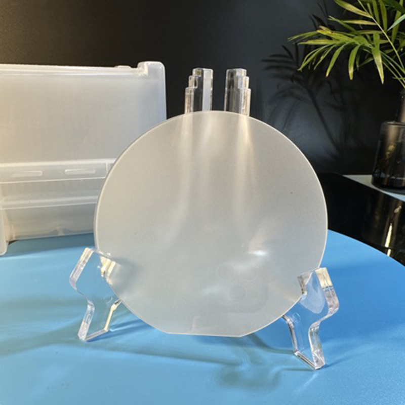
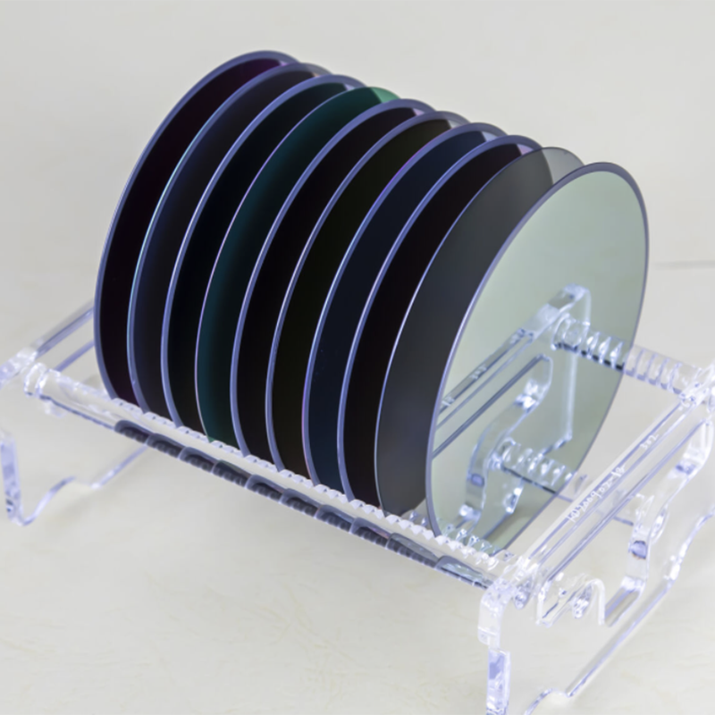
High-Quality Crystal Substrate for Various Industries

By:Admin on 2023-12-11 05:00:05

Gsgg Crystal Substrate Breakthrough: A Game-Changer in Semiconductor IndustryIn a groundbreaking development, a leading semiconductor company has introduced a new Gsgg crystal substrate, which is set to revolutionize the semiconductor industry. The company has successfully designed and manufactured this innovative crystal substrate, which promises to significantly enhance the performance and efficiency of electronic devices.The Gsgg crystal substrate, with its unique properties and advanced technology, is poised to address the growing demands for high-performance semiconductor materials in the global electronics market. Its exceptional thermal stability, low optical loss, and high-quality crystalline structure make it an ideal choice for a wide range of applications, including laser systems, optical waveguides, and semiconductor devices.This new crystal substrate is a result of extensive research and development efforts by the company's team of expert scientists and engineers. Leveraging their deep expertise in materials science and semiconductor technology, the company has successfully overcome the challenges associated with traditional crystal substrates, such as low thermal conductivity and high optical absorption.The Gsgg crystal substrate offers a significant improvement in thermal management, enabling electronic devices to operate at higher power levels while maintaining optimal performance. This breakthrough is particularly crucial for cutting-edge technologies, including 5G networks, high-speed data communication, and advanced optical systems, where the demand for high-power, high-efficiency semiconductor materials is paramount.Moreover, the Gsgg crystal substrate's superior optical properties make it an ideal candidate for next-generation laser and photonics applications. Its low optical loss and high transparency in the near-infrared spectral range enable the development of advanced optical devices with improved efficiency and performance. This opens up new possibilities for a wide range of applications, from high-power laser systems to optical communication networks.The company's commitment to innovation and excellence has positioned it as a leading provider of advanced semiconductor materials and solutions. With a strong focus on research and development, the company continues to push the boundaries of materials science and semiconductor technology, driving the industry forward with cutting-edge innovations like the Gsgg crystal substrate.Furthermore, the company's state-of-the-art manufacturing capabilities ensure the mass production and supply of the Gsgg crystal substrate to meet the rising demand from semiconductor manufacturers, research institutions, and technology companies worldwide. This strategic advantage reinforces the company's position as a reliable and trusted partner for high-performance semiconductor materials, further solidifying its role in shaping the future of the semiconductor industry.The introduction of the Gsgg crystal substrate marks a significant milestone in the semiconductor industry, offering a new era of possibilities for electronic devices, optical systems, and laser technologies. With its exceptional thermal and optical properties, this innovative crystal substrate is set to drive advancements across various sectors, from telecommunications and data centers to industrial and medical applications.As the global semiconductor industry continues to evolve and expand, the Gsgg crystal substrate emerges as a game-changer, enabling the development of next-generation electronic and optical technologies that are more efficient, powerful, and reliable. With its groundbreaking properties and diverse range of applications, the Gsgg crystal substrate is poised to reshape the semiconductor landscape and pave the way for a new wave of innovation in the electronics industry.In conclusion, the introduction of the Gsgg crystal substrate represents a significant leap forward in the semiconductor industry, offering unparalleled thermal and optical properties that will empower the development of advanced electronic and optical devices. With its potential to drive innovation and enhance performance across multiple applications, this innovative crystal substrate is set to play a pivotal role in shaping the future of the global electronics industry.

Read More

High-quality sapphire wafers for advanced technology applications

By:Admin on 2023-12-04 04:36:19

Sapphire wafers are changing the game in the technology world with their unique properties and applications. These wafers are made of sapphire, a crystalline form of aluminum oxide, and are increasingly being used in various industries for their exceptional durability and transparency.The use of sapphire in semiconductor manufacturing is growing rapidly due to its high thermal conductivity, electrical insulation, and resistance to wear and corrosion. This makes sapphire wafers an ideal material for applications such as LED production, consumer electronics, and industrial machinery.One company at the forefront of sapphire wafer production is a leading manufacturer in the semiconductor industry. With state-of-the-art facilities and a team of experts, they are able to produce high-quality sapphire wafers that meet the demanding requirements of their clients. These wafers are used in a wide range of applications, including advanced LED production, optical windows, and semiconductor components.Sapphire wafers are an essential component in the production of LEDs, which are becoming increasingly popular due to their energy efficiency and long lifespan. The unique properties of sapphire, such as its high light transmission and thermal conductivity, make it the material of choice for LED manufacturers. As the demand for LED lighting grows, so does the need for high-quality sapphire wafers, and this company is well-positioned to meet this growing demand.In addition to LED production, sapphire wafers are also used in consumer electronics, such as smartphones and tablets. The scratch-resistant nature of sapphire makes it an ideal material for protective screens, camera lenses, and other components that require durability and high optical quality. This company is a key supplier of sapphire wafers to the consumer electronics industry, providing their clients with the highest quality products for their devices.Furthermore, sapphire wafers are also used in industrial machinery and equipment, where durability and reliability are crucial. The high mechanical strength and chemical resistance of sapphire make it an excellent choice for applications such as bearings, seals, and other critical components. This company's sapphire wafers are used in a wide range of industrial applications, where they have earned a reputation for their exceptional performance and reliability.With their commitment to quality and innovation, this company is driving the advancement of sapphire wafer technology and expanding the possibilities for its use in various industries. Their continued investment in research and development ensures that they stay at the forefront of sapphire wafer production, providing their clients with cutting-edge solutions for their technical challenges.In conclusion, the use of sapphire wafers is revolutionizing the technology industry, and this company is playing a key role in this transformation. With their high-quality sapphire wafers and commitment to innovation, they are enabling their clients to push the boundaries of what is possible in LED production, consumer electronics, and industrial applications. As the demand for sapphire wafers continues to grow, this company is well-equipped to meet this demand and drive the future of sapphire technology.

Read More

Breaking Down the Innovative Gaas Structure: A Game-Changer in Technology

By:Admin on 2023-11-27 04:42:44

Title: Groundbreaking Gaas Structure Revolutionizes the Semiconductor IndustryIntroduction:In a major development that is set to reshape the semiconductor industry, a revolutionary Gaas Structure (need to remove brand name), developed by an innovative company, has been unveiled. This groundbreaking technology promises to overcome the limitations of traditional semiconductor materials, ushering in a new era of enhanced performance and efficiency for electronic devices. With its countless applications across various industries, the Gaas Structure is expected to redefine the way we interact with technology.1. Understanding Gaas Structure:The Gaas Structure, short for Gallium Arsenide Structure, represents a paradigm shift in the field of semiconductor materials. By replacing traditional silicon with gallium arsenide, this groundbreaking technology unlocks unparalleled capabilities. The Gaas Structure is capable of operating at higher frequencies, enabling faster data processing, reduced energy consumption, and improved device performance overall. In addition, this structure is highly versatile, making it suitable for diverse applications, such as telecommunications, aerospace, and automotive industries.2. Advantages and Applications:One key advantage of the Gaas Structure is its high electron mobility, which allows for faster electron movement. This results in exceptionally quick data transfer speeds, making it ideal for high-speed communication devices like 5G infrastructure and satellite communication systems. Moreover, the Gaas Structure offers superior power handling capabilities, enabling the development of more robust and efficient power amplifiers for wireless communication applications.Beyond communication technology, the Gaas Structure finds applications in various other industries. In the aerospace sector, it enables the production of lightweight, high-performance transistors for space exploration, satellite communication, and radar systems. The automotive industry also stands to benefit from this technology, as it allows for the creation of high-speed, low-power electronic systems, improving vehicle safety, infotainment, and powertrain efficiency.3. Company Background:The company behind Gaas Structure (need to remove brand name) is renowned for its expertise in cutting-edge semiconductor technologies. Focused on research and development, the company has a track record of delivering disruptive solutions that address the industry's most pressing challenges. By leveraging their deep understanding of material sciences and semiconductor fabrication, the company has positioned itself as a leader in the field, constantly pushing the boundaries of technology.4. Collaboration and Impact:The Gaas Structure has been the result of extensive collaboration between industry stakeholders, including semiconductor manufacturers, researchers, and device developers. Through joint efforts, the technology has undergone rigorous testing and fine-tuning to ensure its viability and effectiveness. The collective aim is to drive innovation across various sectors, making electronic devices smaller, faster, and more energy-efficient.The implications of this revolutionary technology are far-reaching. By enabling more powerful and energy-efficient electronic systems, the Gaas Structure will contribute to the advancement of autonomous vehicles, wearable technology, IoT devices, and renewable energy systems, among others. Moreover, its adoption will also help address the growing demand for high-speed internet, allowing for seamless streaming and faster data transfer capabilities.Conclusion:With its unprecedented capabilities and potential applications, the Gaas Structure (need to remove brand name) represents a significant leap forward for the semiconductor industry. By harnessing the power of gallium arsenide, this groundbreaking technology promises to revolutionize electronic devices across various sectors. As collaborations continue and further advancements are made, we can expect the Gaas Structure to enhance our everyday lives, driving us into a more connected, efficient, and technologically advanced future.

Read More