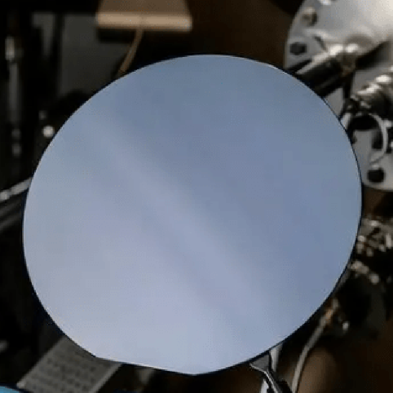
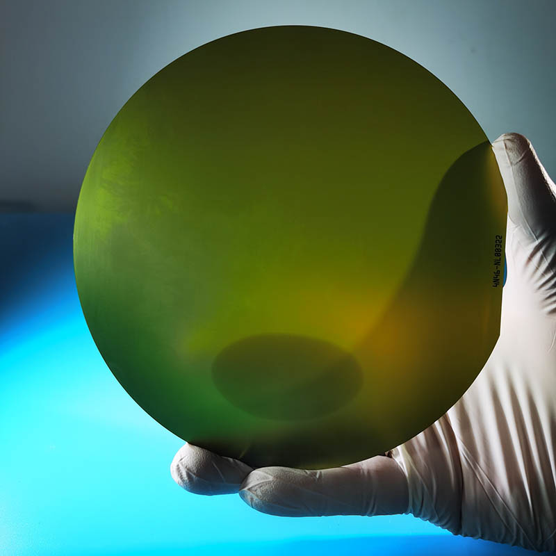
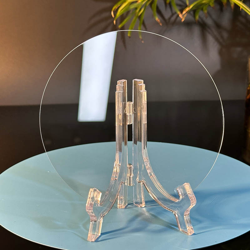
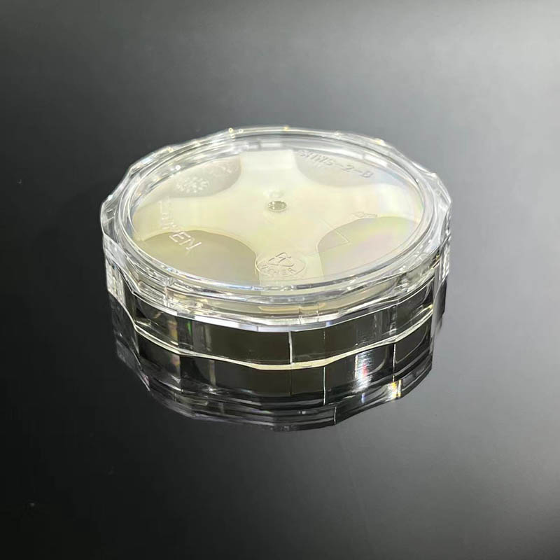
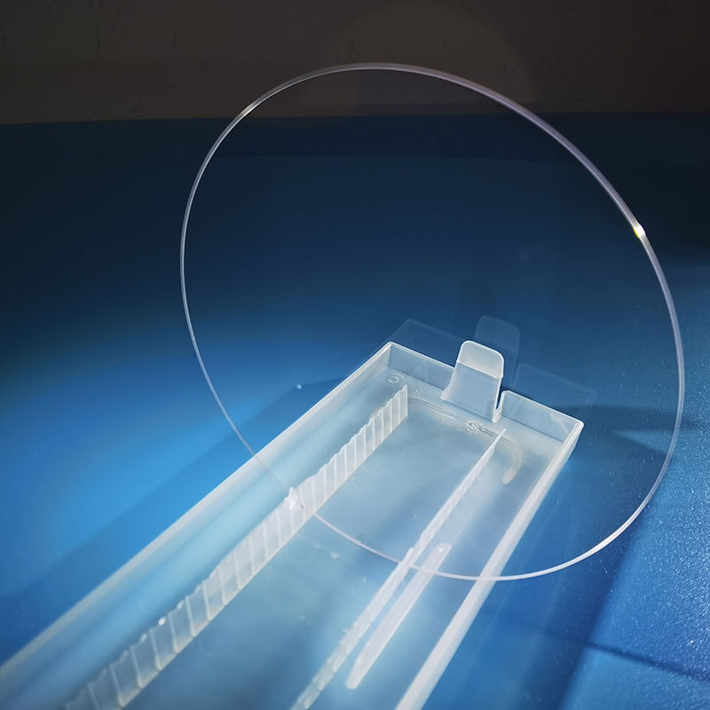
The 6-inch silicon carbide single crystal substrate plays a crucial role in multiple industries. Firstly, it is widely used in the semiconductor industry for the fabrication of high-power electronic devices such as power transistors, integrated circuits, and power modules. Its high thermal conductivity and high-temperature resistance enable better heat dissipation, resulting in improved efficiency and reliability. Secondly, silicon carbide wafers are essential in research fields for the development of new materials and devices. Additionally, the silicon carbide wafer finds extensive applications in the field of optoelectronics, including the manufacturing of LEDs and laser diodes. The 6-inch silicon carbide single crystal substrate has a diameter of 6 inches (approximately 152.4 mm). The surface roughness is Ra < 0.5 nm, and the thickness is 600 ± 25 μm. The substrate can be customized with either N-type or P-type conductivity, based on customer requirements. Moreover, it exhibits exceptional mechanical stability, capable of withstanding pressure and vibration.
The 6-inch silicon carbide single crystal substrate is a high-performance material widely used in the semiconductor, research, andoptoelectronics industries. It offers excellent thermal conductivity, mechanical stability, and high-temperature resistance, making itsuitable for the fabrication of high-power electronic devices and new material research. We provide various specifications andcustomization options to meet diverse customer demands. Contact us for more details on silicon carbide wafers!

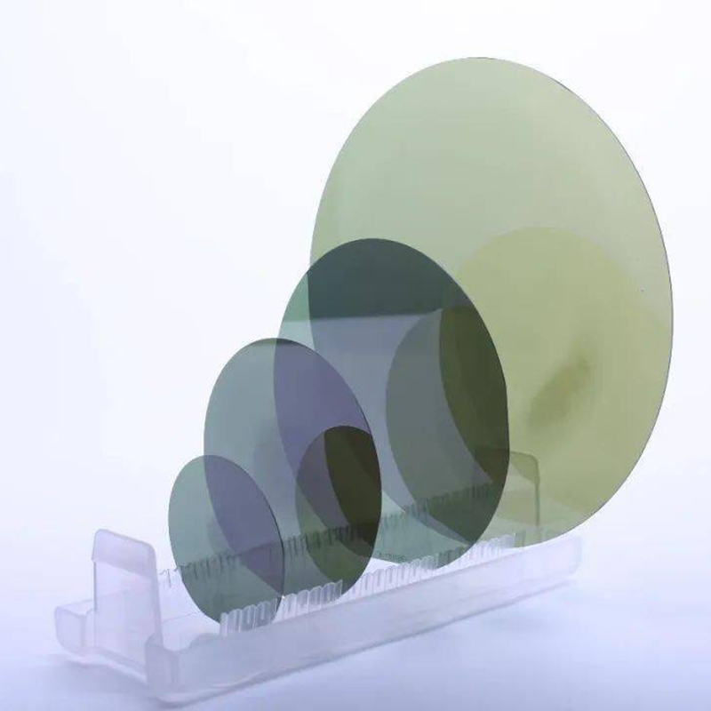


 The 6-inch silicon carbide single crystal substrate has a diameter of 6 inches (approximately 152.4 mm). The surface roughness is Ra < 0.5 nm, and the thickness is 600 ± 25 μm. The substrate can be customized with either N-type or P-type conductivity, based on customer requirements. Moreover, it exhibits exceptional mechanical stability, capable of withstanding pressure and vibration.