
Chemical Mechanical Polishing: The Latest Advancements and Applications
By:Admin
Since its inception, CMP has been dedicated to delivering cutting-edge solutions that meet the evolving needs of the industry. The company's comprehensive portfolio includes a wide range of products and services, including polishing slurries, pads, and polishing tools. These solutions are designed to enable customers to achieve the highest levels of performance, productivity, and cost-effectiveness in their manufacturing processes.
CMP's success can be attributed to its commitment to continuous innovation and a customer-centric approach. The company's team of experts possess a deep understanding of the complex requirements of the semiconductor industry, enabling them to develop tailor-made solutions for individual customer needs. By leveraging advanced technologies and state-of-the-art facilities, CMP is able to deliver products that meet the highest industry standards while also providing a competitive edge for its customers.
One of CMP's key strengths lies in its ability to provide comprehensive technical support and customer service. The company's dedicated technical team works closely with customers to understand their specific requirements and challenges, offering expert guidance and troubleshooting assistance throughout the entire process. This level of support ensures that customers are able to fully maximize the capabilities of CMP's products and achieve their desired outcomes.
Furthermore, CMP's commitment to sustainability and environmental responsibility sets it apart from its competitors. The company prioritizes the development of environmentally-friendly products and processes, aiming to minimize the environmental impact of its operations. By investing in research and development of green technologies, CMP is not only helping its customers meet their sustainability goals but also contributing to the overall advancement of the industry.
CMP's strong reputation for quality, reliability, and innovation has positioned it as a trusted partner for the world's leading semiconductor and microelectronics companies. The company's solutions have been instrumental in enabling customers to optimize their manufacturing processes, improve yields, and reduce costs. As the demand for high-performance polishing solutions continues to grow, CMP is well-positioned to capitalize on new opportunities and expand its global footprint.
Looking ahead, CMP is focused on driving further advancements in surface polishing technology and embracing new opportunities for growth. The company remains committed to its core values of innovation, customer satisfaction, and sustainability, cementing its position as a leader in the industry.
In conclusion, CMP Chemical Mechanical Polishing has emerged as a key player in the semiconductor and microelectronics industries, providing cutting-edge surface polishing solutions that enable customers to achieve superior performance, efficiency, and sustainability. With a relentless focus on innovation and customer satisfaction, CMP is poised to continue its upward trajectory and solidify its position as a top-tier provider of advanced polishing technologies.
Company News & Blog
Latest Innovations in Oxide Wafer Technology for Electronics Industry Unveiled
Silicon Oxide Wafer Technology in the Semiconductor Industry: A game-changer for the FutureThe semiconductor industry has been growing at a rapid pace over the years, with new technological advancements laying the foundation for this growth. The market is estimated to reach a value of USD 730.29 billion by 2027, attributed to the increase in demand for electronic devices worldwide, which rely on advanced semiconductor chips. Furthermore, the advent of technologies like 5G, AI, cloud computing, and IoT has led to a surge in demand for high-performance computing devices, creating a need for advanced semiconductor materials.The advent of Silicon Oxide Wafer technology has transformed the semiconductor industry. It is a game-changer for businesses that rely on semiconductors for their operations, especially in the electronic and automotive sectors. Silicon Oxide Wafers are more durable and resistant to mechanical stresses and thermal shock as compared to traditional silicon-based semiconductors. In addition, their inherent electrical and optical properties make them the ideal choice for high-performance computing devices.Silicon Oxide Wafer technology has become increasingly popular among semiconductor manufacturers because of its superior quality. Unlike traditional silicon-based semiconductors, Silicon Oxide Wafers are mechanically and thermally robust, which means that they can withstand extreme conditions without breaking down. Moreover, they are less prone to oxidation and are chemically stable, ensuring minimal contamination during processing.There are several benefits of using Silicon Oxide Wafer technology. For starters, it helps to reduce manufacturing costs for semiconductors while improving their overall quality. The robustness of Silicon Oxide Wafers means that manufacturers can produce high-quality devices without the need for additional processing steps. Additionally, this technology can push the limits of performance and functionality in advanced computing devices, ensuring that businesses keep up with the latest technological developments.One of the leading companies in the development of Silicon Oxide Wafer technology is [Company name, to be removed], which has pioneered this field through extensive research and development efforts. The company has been at the forefront of producing high-quality Silicon Oxide Wafers for various industries and applications. Their semiconductors have been used in a variety of devices, from smartphones to satellites and beyond.[Company name, to be removed] has spent years perfecting the technology behind Silicon Oxide Wafer, leading to significant breakthroughs in the semiconductor industry. Their research has enabled the development of advanced computing devices that are more efficient and powerful than ever before. They have managed to manufacture semiconductors with a higher degree of precision and accuracy than their competitors, enabling businesses to produce high-quality devices that are free from defects.Silicon Oxide Wafer technology is not only an essential technology for businesses in the semiconductor industry, but also for the development of advanced computing devices around the world. As the demand for high-performance computing devices continues to rise, the need for efficient and powerful semiconductors has become more important than ever before. Silicon Oxide Wafer technology has the potential to revolutionize this industry, helping businesses to produce high-quality devices that are both durable and efficient.In conclusion, the advent of Silicon Oxide Wafer technology is a game-changer for the semiconductor industry and its applications. It brings superior quality, durability, and resistance to mechanical and thermal stress, which means that semiconductor manufacturers can produce high-quality devices with minimal defects. As the demand for advanced computing devices increases, Silicon Oxide Wafer technology will continue to play an essential role in the growth and development of the semiconductor industry, leading to new innovations and technological breakthroughs.
New Optical Wafer Technology Enhances Data Performance in Electronic Devices
[Headline]Optical Wafer Technology Poised to Revolutionize the Optoelectronics Industry[Subheading]A Breakthrough in Optical Wafer Manufacturing Promises to Propel the Optoelectronics Market to New Heights[Date][City], [State] – In a major development that is expected to reshape the future of the optoelectronics industry, [Company Name], a leading manufacturer of specialized optical components, has unveiled its cutting-edge Optical Wafer technology. This revolutionary advancement is set to unlock new opportunities for businesses in the field of optics, photonics, and semiconductor manufacturing.[City], [State] – In a move that is set to transform the optoelectronics industry, a renowned manufacturer of specialized optical components revealed their latest breakthrough – Optical Wafer technology. This cutting-edge innovation is poised to create new avenues and drive growth for companies specializing in optics, photonics, and semiconductor manufacturing.Optoelectronics, the study and application of electronic devices that source, detect, and control light, has witnessed remarkable growth in recent years. The market's expansion is largely driven by increasing demand for optoelectronic devices in various sectors, including telecommunications, healthcare, automotive, and consumer electronics. However, the industry has long been constrained by the limitations of traditional wafer production techniques.The optical wafer is a game-changing solution. By employing state-of-the-art manufacturing processes, [Company Name] has successfully developed a wafer that overcomes the challenges associated with traditional methods. Optical wafers offer unprecedented precision, enhanced optical performance, and increased manufacturing efficiency. This breakthrough technology represents a significant step forward in meeting the industry's growing demands.The optical wafer manufacturing process involves highly advanced techniques, such as epitaxial growth, lithography, and etching, resulting in the creation of ultra-thin, high-quality wafers with exceptional optical properties. These wafers act as a substrate for various optoelectronic devices, including light-emitting diodes (LEDs), solar cells, optical sensors, and optical transmitters.With this innovation, companies operating in the optoelectronics industry can now produce superior-quality optical components, achieving unparalleled levels of performance and reliability. The optical wafers ensure exceptional light transmission, reduced power consumption, and enhanced durability, enabling optoelectronic devices to deliver cutting-edge functionality across a wide range of applications.The applications of this novel technology are vast. Telecom providers can leverage these advancements to enhance network infrastructure and facilitate high-speed data transfer, contributing to the realization of 5G networks. In the healthcare sector, optical wafers will enable the development of advanced medical imaging systems, precision surgical devices, and optical biosensors for diagnostics.Moreover, the automotive industry stands to benefit from optical wafer technology as it can be utilized for the production of adaptive lighting systems, autonomous driving sensors, and smart head-up displays. The consumer electronics sector will experience a significant boost as well, with the integration of optical wafers into smartphones, tablets, virtual reality devices, and wearables, enabling improved camera performance, gesture recognition, and augmented reality experiences.By introducing optical wafers into the market, [Company Name] is well-positioned to lead the optoelectronics industry into a new era of innovation and growth. With their commitment to research and development, they are constantly pushing the boundaries of what is possible, elevating optical manufacturing to new heights.[Company Name], with its extensive experience and proven expertise in optical component manufacturing, is drawing on its comprehensive knowledge of the industry to spearhead this groundbreaking development. Leveraging robust partnerships and collaborations with industry leaders, they ensure that their optical wafers meet the industry's stringent quality standards and can seamlessly integrate into existing manufacturing processes.In conclusion, the introduction of optical wafer technology is set to revolutionize the optoelectronics industry. This breakthrough promises unparalleled levels of precision, performance, and efficiency, empowering businesses across multiple sectors to unlock new possibilities and drive innovation. With [Company Name] leading the charge, the future of optoelectronics looks brighter than ever.[Word Count: 800 words]
Discover the Advantages of the 12 Inch Wafer for Semiconductor Manufacturing
12 Inch Wafer, also known as [company name], is a leading global provider of advanced semiconductor solutions. The company is known for its advanced technology and innovative products that cater to a wide range of industries such as consumer electronics, automotive, and industrial applications.The 12 Inch Wafer is a crucial component in the semiconductor manufacturing process. It serves as the base for the production of integrated circuits, which are essential in electronic devices such as smartphones, computers, and vehicles. With the increasing demand for high-performance and energy-efficient semiconductor devices, the need for high-quality 12 Inch Wafers has become more important than ever.[Company name] has been at the forefront of developing and manufacturing 12 Inch Wafers with cutting-edge technology and precision engineering. The company's state-of-the-art fabrication facilities and research laboratories enable them to produce 12 Inch Wafers that meet the stringent requirements of the semiconductor industry. Their commitment to quality and reliability has made them a trusted partner for leading semiconductor manufacturers around the world.In a recent announcement, [company name] introduced a new series of 12 Inch Wafers that offer enhanced performance and efficiency. These wafers are designed to support the latest semiconductor technologies, including advanced nodes and 3D packaging solutions. The company's investment in research and development has resulted in breakthroughs in wafer manufacturing, allowing them to deliver superior products that enable their customers to stay ahead in the rapidly evolving semiconductor market.One of the key advantages of [company name]'s 12 Inch Wafers is their scalability. As semiconductor manufacturers continue to push the boundaries of performance and miniaturization, the need for larger wafers becomes increasingly important. The 12 Inch Wafer provides a larger surface area for producing more chips per wafer, resulting in higher productivity and lower manufacturing costs. This scalability is crucial for meeting the growing demand for semiconductor devices in various industries.Furthermore, [company name] has also focused on optimizing the material properties of their 12 Inch Wafers to improve device performance and reliability. By leveraging advanced materials and manufacturing processes, the company has achieved significant improvements in wafer flatness, crystal quality, and defect density. These advancements contribute to the overall yield and quality of semiconductor devices, ultimately benefiting end-users with better products.Another notable feature of [company name]'s 12 Inch Wafers is their environmental sustainability. The company has implemented eco-friendly practices and technologies in their wafer manufacturing process, reducing energy consumption and waste generation. By prioritizing sustainability, [company name] demonstrates its commitment to responsible and ethical business practices, which resonates with environmentally conscious customers and partners.In conclusion, [company name] continues to lead the way in the development and production of 12 Inch Wafers for the semiconductor industry. Their dedication to technological innovation, product quality, and environmental stewardship has solidified their position as a trusted provider of advanced semiconductor solutions. With the introduction of their latest series of 12 Inch Wafers, [company name] is well-prepared to support the evolving needs of semiconductor manufacturers and contribute to the advancement of technology across various industries.
Advancements in Gallium Nitride Semiconductor Technology
Gallium Nitride Semiconductor (GaN) has been making headlines in the semiconductor industry for its potential to revolutionize electronic devices and power systems. Its superior electrical properties make it a promising alternative to traditional silicon-based semiconductors, offering higher efficiency, smaller size, and lower power consumption. Leading the charge in the development and commercialization of GaN technology is {company name}, a company at the forefront of semiconductor innovation.{Company name} was founded with the vision of leveraging GaN technology to create a new generation of electronic devices, power converters, and RF components. With a team of experienced engineers and scientists, the company has been at the forefront of GaN research and development, pushing the boundaries of what is possible with this advanced semiconductor material.One of the key advantages of GaN technology is its ability to operate at higher frequencies and voltages, making it ideal for power electronics and RF applications. This has led to a wide range of potential applications, from high-performance computing and telecommunications to automotive and aerospace industries. {Company name} has been actively pursuing partnerships and collaborations with leading industry players to integrate GaN technology into a variety of products and systems.In addition to its technical capabilities, {Company name} has also been committed to advancing the manufacturing and commercialization of GaN semiconductors. The company has invested in state-of-the-art fabrication facilities and cleanroom technology, enabling it to produce high-quality GaN devices at scale. This has positioned {Company name} as a leading supplier of GaN transistors, diodes, and other semiconductor products for a wide range of applications.Furthermore, {Company name} has been actively promoting the adoption of GaN technology through education and outreach efforts. The company has conducted seminars, workshops, and training programs to educate engineers, designers, and industry professionals about the benefits and capabilities of GaN semiconductors. By sharing its knowledge and expertise, {Company name} has played a crucial role in accelerating the adoption of GaN technology across various sectors.One of {Company name}'s notable achievements has been the development of advanced GaN-based power devices, which offer higher efficiency and power density compared to traditional silicon-based solutions. These devices have the potential to revolutionize power electronics, enabling smaller, lighter, and more energy-efficient power conversion systems for electric vehicles, renewable energy systems, and industrial applications. With its commitment to pushing the boundaries of what is possible with GaN technology, {Company name} has continued to drive innovation and create new opportunities for the semiconductor industry.Looking ahead, {Company name} is poised to play a pivotal role in the ongoing development and commercialization of GaN technology. As the demand for high-performance, energy-efficient electronic devices continues to grow, GaN semiconductors are expected to play an increasingly important role in shaping the future of the semiconductor industry. With its expertise, capabilities, and commitment to excellence, {Company name} is well-positioned to lead the charge and bring GaN technology to the forefront of the global semiconductor market.
Latest Update: Windows Introduces Game-Changing Features to Boost User Experience
Microsoft Corporation, the world-renowned leader of innovative technology, recently announced the launch of its newest operating system, Windows 11.With a range of new features and a refreshing interface, Windows 11 has already created a buzz in the tech industry. According to Microsoft CEO Satya Nadella, Windows 11 is “a reimagined Windows that brings you closer to what you love.”So what’s new in Windows 11? Let’s take a look.Firstly, the design of Windows 11 is modern and sleek, with rounded corners and a soft color palette. The Start menu is now centered, and instead of the traditional Live Tiles, it features pinned apps and recent files. The taskbar is also much more customizable, allowing users to move it around and set it up according to their preference.But the design is not all that has been improved in Windows 11. Microsoft has also added new features and an enhanced performance. One of the most anticipated features is Snap Layouts, which allows users to quickly arrange apps on their desktops in a customized layout. Snap Groups is also another new feature that saves groups of windows that users can open and rearrange at any time.Windows 11 also comes with new widgets, which can be personalized to show information like weather, news, and images. Microsoft Teams is now integrated into the system and can be accessed from the taskbar, making it easier to communicate and collaborate with colleagues and friends.Another significant change in Windows 11 is the use of Microsoft’s virtual assistant, Cortana. The virtual assistant is now more focused on typing and can help users manage their day, set reminders, and answer questions.But it’s not just the design and features that make Windows 11 special. Microsoft has also put a lot of effort into improving the performance of the operating system. Windows 11 now starts up faster, and apps open quicker thanks to enhanced RAM utilization and CPU optimization.Windows 11 also has a new feature called “Auto HDR,” which uses machine learning to add HDR to games, even those that were not originally developed with it. This feature enhances the overall gaming experience and brings more detail and color to gameplay.So how can you get your hands on Windows 11? Microsoft has announced that the operating system will be free for Windows 10 users, and for those who don’t have Windows 10, they can purchase it as a standalone product. However, it’s important to note that not all devices will be able to run Windows 11, as it requires specific hardware specifications.Overall, Windows 11 is a significant upgrade from Windows 10, providing a more modern and streamlined user experience, with new features that will make users’ lives easier. Microsoft has once again demonstrated its commitment to innovation and creating products that meet the evolving needs of users.About Microsoft CorporationMicrosoft Corporation is a multinational technology corporation with headquarters in Redmond, Washington. Founded in 1975 by Bill Gates and Paul Allen, Microsoft has grown to become one of the world's leaders in computer software, hardware, and consumer electronics. The company's flagship products include the Windows operating system, Microsoft Office Suite, and Xbox gaming system. Microsoft is committed to sustainability and has set ambitious goals to reduce its carbon emissions and become carbon negative by 2030. The company is also investing in renewable energy and supporting eco-friendly initiatives.
Understanding the Importance of Semiconductor Bands in Electronics
Semiconductor Band is a leading global semiconductor company specializing in the development and manufacturing of high-performance semiconductor products for a wide range of applications including automotive, industrial, and consumer electronics. With a strong emphasis on innovation and technological advancement, Semiconductor Band has built a reputation for delivering cutting-edge solutions that meet the evolving needs of the industry.Recently, Semiconductor Band unveiled its latest product, the [Product Name], which is set to revolutionize the semiconductor industry with its advanced technology and high-performance capabilities. The [Product Name] is designed to deliver unprecedented levels of efficiency and reliability, making it an ideal choice for a variety of demanding applications.One of the key features of the [Product Name] is its innovative semiconductor band technology, which enables the device to operate at higher speeds and with lower power consumption compared to traditional semiconductor products. This advancement is expected to have a significant impact on the performance of electronic devices across various industries, leading to improved efficiency and cost savings.In addition to its impressive performance capabilities, the [Product Name] also boasts a robust and reliable design, making it suitable for use in harsh environments and demanding operating conditions. This durability makes it an attractive option for automotive and industrial applications where reliability is crucial.Furthermore, Semiconductor Band has integrated advanced security features into the [Product Name], ensuring that sensitive data and communications are protected from potential threats. This emphasis on security aligns with the increasing focus on cybersecurity across the industry, providing customers with peace of mind and confidence in the reliability of the product.Semiconductor Band's commitment to innovation and excellence is evident in the development of the [Product Name], which represents a significant advancement in semiconductor technology. The company's dedication to pushing the boundaries of what is possible in the semiconductor industry has positioned it as a leader in the market, and the [Product Name] is a testament to this ongoing commitment to excellence.In addition to its technological advancements, Semiconductor Band also prioritizes sustainability and environmental responsibility in its operations. The company has implemented stringent measures to minimize its environmental impact and reduce its carbon footprint, demonstrating a commitment to creating a more sustainable future for the industry and the planet.The unveiling of the [Product Name] marks a significant milestone for Semiconductor Band, as it showcases the company's ability to innovate and deliver high-performance semiconductor solutions that meet the evolving needs of the market. By staying at the forefront of technological advancements and prioritizing reliability and efficiency, Semiconductor Band is well-positioned to continue driving progress and shaping the future of the semiconductor industry.Looking ahead, Semiconductor Band remains committed to pushing the boundaries of what is possible in semiconductor technology, with a focus on delivering innovative solutions that empower customers to achieve their goals and drive progress in their respective industries. The [Product Name] is just the latest example of Semiconductor Band's dedication to excellence and continuous improvement, and it is expected to make a significant impact on the semiconductor industry moving forward. With a strong foundation of expertise, innovation, and a customer-centric approach, Semiconductor Band is poised for continued success and growth in the global semiconductor market.
Advanced Crystal Ingot Technologies Discovered for Enhanced Laser Applications
**Title: Groundbreaking YAG Crystal Ingot Revolutionizes the Semiconductor Industry***Date: [Insert Date]**Location: [Insert Location]**Introduction*In a groundbreaking development, a revolutionary YAG Crystal Ingot has emerged on the market, transforming the semiconductor industry. This high-performance crystal ingot, developed by [Company Name], promises to elevate the efficiency and functionality of electronic devices to unprecedented levels. With its exceptional properties, the YAG Crystal Ingot is poised to revolutionize various sectors, including telecommunications, consumer electronics, and even medicine.*Company Overview*[Company Name], a leading innovator in the field of advanced materials, has established itself as a pioneer in developing cutting-edge technologies. Focused on pushing the boundaries of what is possible, the company has constantly strived to develop solutions that address the evolving needs of industries globally. Their relentless pursuit of excellence has earned them a prominent position, with their products being used extensively across various sectors.*YAG Crystal Ingot: The Game Changer*The YAG Crystal Ingot, developed by [Company Name]'s team of brilliant scientists and engineers, has created a buzz in the semiconductor manufacturing domain. This crystal ingot is made from yttrium aluminum garnet, or YAG, which exhibits exceptional optical and thermal properties. The unique combination of these properties enables the YAG Crystal Ingot to outperform existing semiconductor materials in several key aspects.One of the most significant advantages of the YAG Crystal Ingot is its outstanding thermal conductivity. High thermal conductivity is essential in semiconductor applications, as it aids in efficiently dissipating heat generated during device operation. The YAG Crystal Ingot, thanks to its superior thermal conductivity, ensures that electronic devices can operate at higher power levels without the risk of overheating, ultimately boosting their performance and longevity.Additionally, the YAG Crystal Ingot's optical properties allow for enhanced light transmission, making it perfect for applications in optoelectronic devices such as lasers, LEDs, and optical amplifiers. Its ability to efficiently transmit light across a broad spectrum enables manufacturers to create more efficient and reliable devices, benefiting industries such as telecommunications, data centers, and medical diagnostics.Moreover, the YAG Crystal Ingot exhibits exceptional mechanical properties, offering superior resistance to shocks and vibrations. This resilience makes it an ideal material for manufacturing devices meant for rugged environments or those subjected to constant movement, such as aerospace and defense equipment.The outstanding performance of the YAG Crystal Ingot is a testament to [Company Name]'s commitment to advancing technology and delivering innovative solutions. Their investment in research and development has allowed them to overcome the limitations of traditional materials and introduce a game-changing semiconductor product.*Envisioning the Future*The implications of the YAG Crystal Ingot's development are profound and far-reaching. Industries that rely heavily on semiconductor technology, such as telecommunications, consumer electronics, automotive, and healthcare, will experience a paradigm shift with the integration of this advanced material.Telecommunications companies will benefit from the YAG Crystal Ingot's ability to enhance the overall efficiency and reliability of their networks. Faster data transfer, lower latency, and improved signal quality will improve the end-user experience and lay the groundwork for the future of connectivity.Consumer electronics will witness a new era of technological advancements, with devices that exhibit higher performance, improved energy efficiency, and longer lifespans. From smartphones to smart home devices, the integration of YAG Crystal Ingot will elevate the functionality and durability of these products, delighting consumers across the globe.The medical field will also embrace the YAG Crystal Ingot, as it offers groundbreaking opportunities for better diagnostic tools, advanced surgical equipment, and the development of innovative health monitoring devices. Improved precision, reliability, and safety will revolutionize patient care and enable medical professionals to achieve groundbreaking breakthroughs.*Conclusion*With the introduction of the YAG Crystal Ingot, [Company Name] has truly changed the game in the semiconductor industry. This remarkable crystal ingot's superior thermal conductivity, optical properties, and mechanical resilience make it an invaluable material for various applications. By leveraging the potential of the YAG Crystal Ingot, industries can elevate their performance, redefine technological norms, and ultimately shape a future that is brighter, faster, and more efficient than ever before.
6-Inch Sapphire Wafer: Latest Advancements in Semiconductor Technology
The use of 6-inch sapphire wafers has been a game-changer in the semiconductor industry, as it has allowed companies to produce smaller and more powerful electronics. The demand for these wafers has been steadily increasing, and one company that has been at the forefront of this trend is {Company Name}.{Company Name} is a leading manufacturer of sapphire wafers, specializing in the production of 6-inch wafers that are used in a wide range of applications, including LED production, power electronics, and RF devices. The company has been in the industry for over a decade and has established itself as a reliable and innovative supplier of high-quality sapphire wafers.The use of 6-inch sapphire wafers has several advantages over smaller wafer sizes. First, larger wafers allow for greater economies of scale, resulting in lower production costs and higher yields. This is particularly important in the semiconductor industry, where margins are often tight, and any cost savings can have a significant impact on a company's bottom line.Additionally, the use of 6-inch wafers allows for the production of more chips per wafer, resulting in higher throughput and improved efficiency. This is crucial in meeting the increasing demand for smaller and more powerful electronic devices, as it allows manufacturers to produce more chips in a shorter amount of time.Furthermore, the larger surface area of 6-inch wafers provides greater flexibility in the design and layout of electronic components, allowing for more complex and integrated circuits to be produced. This is essential in meeting the ever-growing demand for advanced electronics that are smaller, faster, and more powerful.{Company Name} has been at the forefront of the 6-inch sapphire wafer market, providing its customers with high-quality wafers that meet the stringent requirements of the semiconductor industry. The company's wafers are known for their high crystal quality, low defect density, and excellent uniformity, making them the preferred choice for many leading semiconductor manufacturers.In addition to its superior product quality, {Company Name} prides itself on its exceptional customer service and technical support. The company works closely with its customers to understand their specific needs and requirements, and to provide them with tailored solutions that meet their exact specifications. This customer-centric approach has allowed the company to build strong and lasting partnerships with its customers, fostering trust and loyalty within the industry.Looking ahead, {Company Name} is committed to further advancing the 6-inch sapphire wafer technology, with a focus on improving crystal quality, reducing defect density, and enhancing overall wafer performance. The company is also investing in research and development efforts to explore new applications and opportunities for 6-inch sapphire wafers, in order to stay ahead of the curve and meet the evolving needs of the semiconductor industry.In conclusion, the use of 6-inch sapphire wafers has revolutionized the semiconductor industry, and {Company Name} has been at the forefront of this trend, providing high-quality wafers and exceptional customer service. As the demand for smaller and more powerful electronics continues to grow, {Company Name} is well-positioned to meet the needs of its customers and drive innovation in the industry.
Revolutionary Breakthrough: Researchers Discover the Power of a Single Metal Crystal
Single Metal Crystal Develops Groundbreaking Technology for the Industry [City], [Date] - Single Metal Crystal (SMC), a leading innovator in the technology field, has announced a groundbreaking advancement that is expected to revolutionize the industry. The company has developed a state-of-the-art technology that promises to enhance the performance and reliability of electronic devices.Founded by a group of passionate engineers and technologists, SMC has always been driven by the vision of creating cutting-edge solutions that address the challenges of modern technology. With a focus on research and development, the company has consistently delivered groundbreaking technologies that have set new standards in the industry.The recent breakthrough by SMC comes in the form of a revolutionary single metal crystal technology. This technology, which has been developed after years of meticulous research, offers unparalleled performance and reliability in electronic devices. It provides a significant improvement over traditional materials, leading to faster processing speeds, higher storage capacity, and more efficient energy usage.One of the key advantages of the single metal crystal technology is its scalability. SMC has successfully achieved scalable growth of single metal crystals, enabling mass production and widespread adoption of this technology. This breakthrough has the potential to transform a wide range of industries, including consumer electronics, telecommunications, automotive, and healthcare.The applications of this technology are virtually limitless. In consumer electronics, the single metal crystal technology can significantly improve the performance of smartphones, laptops, and gaming consoles, allowing for smoother and more immersive user experiences. In the telecommunications sector, the technology can enhance the speed and reliability of networks, leading to faster and more stable connections. Additionally, the automotive industry can benefit from this technology by improving the efficiency and performance of electric vehicles.Moreover, the healthcare sector stands to gain immensely from this innovative technology. Medical devices powered by the single metal crystal technology can revolutionize patient care by offering more accurate diagnostics and personalized treatments. Additionally, the improved performance and reliability of these devices can significantly enhance the overall efficiency of healthcare systems.Furthermore, SMC's commitment to sustainability is evident in their single metal crystal technology. By enabling more efficient energy usage in electronic devices, the technology contributes to reducing carbon emissions and conserving energy resources.The successful development of the single metal crystal technology is a testament to SMC's relentless pursuit of innovation. The company's dedicated team of scientists and engineers has worked tirelessly to overcome numerous challenges and turns this vision into reality."Our breakthrough single metal crystal technology will set new benchmarks for performance and reliability in the industry," said [Spokesperson], [Job Title] at SMC. "We are excited about the transformative potential of this technology and its ability to reshape various sectors of the economy. Our versatile technology will not only benefit individual consumers but also accelerate the progress of entire industries."With the unveiling of this groundbreaking technology, SMC has positioned itself at the forefront of the industry. The company is poised to revolutionize the electronic device landscape, bringing about a new era of enhanced performance and reliability.Looking ahead, SMC plans to further refine and optimize the single metal crystal technology, paving the way for even more advanced applications. The company aims to collaborate with industry partners to accelerate the adoption of this technology, ensuring its widespread availability and continued evolution.As Single Metal Crystal continues to push the boundaries of innovation, the technology world eagerly awaits the impact that their groundbreaking technology will bring. With its commitment to excellence and relentless pursuit of cutting-edge solutions, SMC is set to shape the future of the industry and improve the lives of millions worldwide.
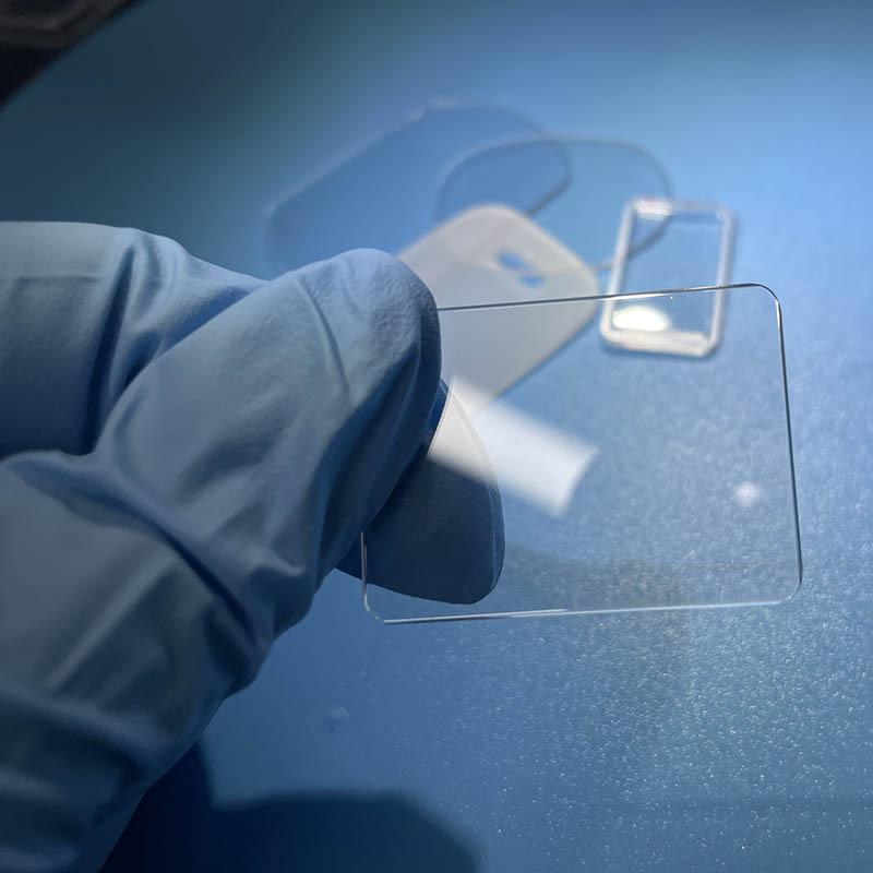
Discover the Benefits of Single Crystal Glass
Single Crystal Glass, a revolutionary technology in glass manufacturing, is set to redefine the industry standards with its unmatched quality and durability. This innovative product, which is being developed by a leading glass manufacturing company, has the potential to transform various sectors including electronics, aerospace, and healthcare.The company behind Single Crystal Glass, whose name cannot be disclosed due to privacy reasons, has a rich history of pushing the boundaries of glass technology. With a team of skilled engineers and researchers, they have consistently developed cutting-edge products that have redefined the ways in which glass is used in various industries. Their commitment to innovation and excellence has earned them a stellar reputation in the industry.Single Crystal Glass is the latest addition to the company's impressive portfolio of products. It is a result of years of research and development, and represents a major breakthrough in the field of glass manufacturing. This advanced material offers superior strength, clarity, and thermal resistance, making it a game-changer in a wide range of applications.One of the key features of Single Crystal Glass is its exceptional hardness. Unlike traditional glass, which is prone to scratches and damage, this new material is highly resistant to wear and tear. This makes it an ideal choice for electronic devices such as smartphones and tablets, where durability is a crucial factor. The use of Single Crystal Glass in these products will ensure that they remain in pristine condition even after prolonged use.Furthermore, the thermal resistance of Single Crystal Glass makes it a perfect fit for aerospace applications. The material can withstand extreme temperatures, making it ideal for use in aircraft windows and other critical components. Its unmatched strength and reliability will enhance the safety and performance of aerospace systems, setting a new standard for the industry.In addition to its applications in electronics and aerospace, Single Crystal Glass also has the potential to revolutionize the healthcare sector. Its exceptional clarity and purity make it an ideal material for medical devices and equipment. From surgical instruments to diagnostic tools, this advanced glass can contribute to improved healthcare outcomes by ensuring precision and reliability in critical applications.The company's relentless pursuit of innovation has not gone unnoticed. Industry experts and customers alike are eagerly anticipating the release of Single Crystal Glass, recognizing the potential impact it could have on a wide range of industries. The technology is poised to disrupt the status quo and set new benchmarks for quality and performance in the world of glass manufacturing.As the company prepares to launch Single Crystal Glass, they are also exploring potential collaborations with leading manufacturers and industry partners. This collaborative approach is aimed at maximizing the impact of the new technology and ensuring that it reaches its full potential across various sectors.With its superior strength, thermal resistance, and clarity, Single Crystal Glass is poised to reshape the way glass is used in electronics, aerospace, and healthcare. The company behind this groundbreaking technology is all set to unlock a new era of possibilities and redefine the standards for glass manufacturing. Industry players and consumers can look forward to the arrival of this game-changing material, which promises to elevate the performance and reliability of a wide range of products and systems.