
Durable and Scratch-Resistant Sapphire Glass: The Future of Advanced Technology
By:Admin
In today's fast-paced and technologically advanced world, the demand for durable and transparent materials has never been higher. As a result, the use of custom sapphire glass has become increasingly popular across a wide range of industries. This remarkable material is not only incredibly robust and scratch-resistant, but it also boasts exceptional optical clarity, making it the ideal choice for a variety of applications.
Custom sapphire glass is a synthetic material that offers superior durability and transparency compared to traditional glass. It is made through a process called crystal growth, in which aluminum oxide is heated to extreme temperatures and then formed into a single crystal. The resulting material is incredibly hard and scratch-resistant, making it ideal for use in applications where durability is a top priority.
One of the leading companies in the production of custom sapphire glass is {Company Name}. With a strong focus on innovation and quality, {Company Name} has established itself as a trusted provider of high-quality sapphire glass products. The company's advanced manufacturing processes and cutting-edge technology allow it to produce custom sapphire glass with exceptional precision and consistency, meeting the ever-growing demand for this versatile material.
{Company Name} offers a wide range of custom sapphire glass products, catering to the diverse needs of its customers. From smartphone screens and camera lenses to watch faces and medical devices, the company's sapphire glass solutions are renowned for their unmatched durability and optical clarity. Furthermore, {Company Name} is committed to providing tailored solutions to meet the specific requirements of its clients, ensuring that every product meets the highest standards of quality and performance.
One of the key advantages of custom sapphire glass is its exceptional scratch resistance. Unlike traditional glass, sapphire glass is virtually impervious to scratches, ensuring that products made with this material maintain their pristine appearance even after prolonged use. This makes it an ideal choice for consumer electronics, where the need for durable and long-lasting displays is paramount.
In addition to its remarkable durability, custom sapphire glass also offers unparalleled transparency. With its superior optical properties, sapphire glass allows for maximum light transmission, resulting in stunningly clear and crisp visuals. This makes it the material of choice for applications where optical clarity is essential, such as high-end camera lenses and premium watch faces.
Furthermore, custom sapphire glass is also highly resistant to harsh environmental factors, such as extreme temperatures and chemical exposure. This makes it an excellent choice for outdoor displays, automotive applications, and industrial equipment, where durability and reliability are crucial.
{Company Name} is dedicated to continually pushing the boundaries of what is possible with custom sapphire glass. Through ongoing research and development efforts, the company is working to expand the potential applications of this remarkable material, opening new doors for innovation across various industries.
It is clear that custom sapphire glass has become the new standard in durability and transparency, offering unmatched performance and reliability in a wide range of applications. With {Company Name} leading the way in the production of high-quality sapphire glass products, the future looks bright for this remarkable material. As the demand for durable and transparent materials continues to grow, custom sapphire glass is poised to play a pivotal role in shaping the technology of tomorrow.
Company News & Blog
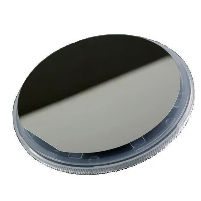
Discover the Benefits of High Resistivity Silicon Wafers for Enhanced Performance
High Resistivity Silicon Wafer Revolutionizes Semiconductor IndustryIn recent news, a groundbreaking technology known as High Resistivity Silicon Wafer has emerged as a game-changer in the semiconductor industry. This innovative solution, developed by a leading company in the field, aims to overcome long-standing challenges and open doors to new possibilities in various applications.The company behind this groundbreaking technology, which prefers to remain anonymous, has a proven track record of excellence in the semiconductor industry. With decades of experience and a dedicated team of experts, their commitment to innovation has led to numerous advancements and breakthroughs.High Resistivity Silicon Wafer, the company's latest invention, has the potential to redefine the semiconductor landscape. By addressing key shortcomings associated with traditional silicon wafers, this technology promises a higher level of performance and efficiency.The primary advantage of the High Resistivity Silicon Wafer lies in its ability to minimize impurities and defects that have plagued conventional wafers. This advancement results in superior electrical properties, allowing for improved device performance and energy efficiency. Furthermore, the reduced presence of impurities enhances the quality and reliability of manufactured semiconductor components.The impact of this breakthrough technology can be felt across a wide range of industries. From consumer electronics and telecommunications to automotive and healthcare, the High Resistivity Silicon Wafer offers unparalleled possibilities. Its high electrical resistance enables the creation of more reliable and sophisticated devices, boosting product performance and enhancing user experiences.One sector that is set to benefit greatly from this innovation is the telecommunications industry. With the ever-increasing demand for faster data transfer and improved wireless communication, the need for high-performance semiconductor components is more significant than ever. The High Resistivity Silicon Wafer enables the development of faster and more reliable communication systems, paving the way for next-generation technologies such as 5G networks.Automotive manufacturers are also poised to benefit from this groundbreaking technology. As the demand for electric vehicles continues to rise, the need for efficient and reliable semiconductors becomes crucial. The High Resistivity Silicon Wafer offers a significant advantage in this regard, enabling the production of more efficient power electronics and driving the future of sustainable transportation.Furthermore, the healthcare industry can leverage the potential of this technology to enhance diagnostics and treatment. With the increasing reliance on medical devices and advancements in technologies such as artificial intelligence and telemedicine, the quality and reliability of semiconductor components are paramount. The High Resistivity Silicon Wafer ensures the production of highly accurate and dependable medical devices, thus revolutionizing patient care.This breakthrough technology is also bringing economic benefits by creating new opportunities in the manufacturing sector. The production of High Resistivity Silicon Wafers necessitates advanced fabrication processes and equipment, leading to the growth of specialized industries and the generation of high-skilled jobs.As we witness the transformative potential of the High Resistivity Silicon Wafer, it is clear that the company behind this innovation is at the forefront of shaping the semiconductor industry. By pushing the boundaries of what is currently possible, they have set a new standard for semiconductor performance and efficiency.The release of this groundbreaking technology marks an exciting chapter in the semiconductor industry. With its vast array of applications and potential to revolutionize multiple sectors, the High Resistivity Silicon Wafer promises a future marked by enhanced device performance, improved energy efficiency, and breakthrough innovations.
Exploring the Growing Demand for Sic Wafers in Technology Industry
Title: Revolutionary Technology Empowers Electronics Industry with Next-Gen Silicon Carbide WafersIntroduction:In an era driven by rapid technological advancements, the global electronics industry seeks reliable and efficient solutions that can accelerate the pace of innovation. Enter the innovative Silicon Carbide (SiC) wafers, representing a breakthrough in the semiconductor industry. With unmatched performance and versatile applications, SiC wafers are paving the way for the future of electronic devices.[Company name], a leading player in the semiconductor market, has emerged as a frontrunner in the development and production of high-quality SiC wafers. Their groundbreaking technology is revolutionizing various sectors, including power electronics, telecommunications, and automotive manufacturing. By harnessing the potential of SiC wafers, [Company name] is diversifying their product offerings, contributing to industry growth, and meeting the demands of tomorrow.Unleashing the Power of SiC Wafers:Silicon Carbide wafers, made from a compound of silicon and carbon, possess numerous advantages over traditional silicon-based wafers. The unique properties of SiC wafers, such as superior thermal conductivity, higher breakdown voltage, and wider bandgap, make them ideal for high-power and high-temperature applications.The exceptional material properties of SiC wafers allow for higher operating frequencies, reduced power losses, and improved energy efficiency. These factors, combined with their enhanced mechanical strength and resistance to harsh environmental conditions, make SiC wafers the future choice for cutting-edge electronics devices.Industries Benefiting from SiC Wafers:1. Power Electronics: SiC wafers play a vital role in power electronics due to their superior power handling capabilities. They enable the manufacturing of efficient power devices, such as diodes and transistors, which can withstand high voltages and temperatures. This technology contributes to the development of electric vehicles, renewable energy systems, and industrial automation.2. Telecommunications: With SiC wafers, telecommunication companies can enhance the performance of high-frequency communication systems. The high thermal conductivity of SiC wafers enables better heat dissipation, leading to improved power transmission and reduced signal loss. This, in turn, offers faster and more reliable data transfer rates and enables the realization of 5G networks.3. Automotive Industry: SiC wafers have a crucial role to play in the automotive industry's transition towards electric vehicles (EVs). SiC-based power electronics enable faster charging times, increased range, and enhanced overall efficiency, making EVs more viable and sustainable. Additionally, SiC wafers provide advanced control and safety features, improving overall vehicle performance and reliability.[Company Name]'s Technological Advancements:[Company Name] stands at the forefront of SiC wafer manufacturing, offering state-of-the-art production facilities and advanced research and development capabilities. Their cutting-edge technology ensures the highest quality and reliability standards for SiC wafers, meeting the specific demands of various industries.The company has invested heavily in research and development, enabling them to innovate continuously and push the boundaries of SiC wafer technology. Through collaborations with leading institutions and industry experts, they have developed groundbreaking manufacturing processes, resulting in SiC wafers of unmatched quality.Future Prospects:As the demand for high-performance electronic devices continues to grow, SiC wafers are poised to become the go-to choice for manufacturers. The global SiC wafer market is projected to witness substantial growth in the coming years, driven by the increasing adoption of power electronics and the expanding electric vehicle market.[Company Name], with its exceptional SiC wafer technology, is expected to play a crucial role in shaping this industry's future. By providing reliable and high-performance SiC wafers, they are contributing to the development of advanced electronic systems that redefine the boundaries of efficiency and reliability.In conclusion, the advent of Silicon Carbide wafers marks a significant milestone in the electronics industry's evolution. [Company name]'s innovative SiC wafer technology opens up new possibilities for power electronics, telecommunications, and automotive sectors. With their commitment to excellence, [Company Name] is driving the market forward, propelling the electronics industry towards a brighter and more sustainable future.
Discover the Versatility and Durability of Zirconium Dioxide (ZrO2) Ceramic
[Title]: Advanced Zro2 Ceramic Revolutionizing Multiple Industries: A Closer Look at its Applications and Company Innovations[Subtitle]: (Remove brand name) Pioneering the Way With Zro2 Ceramic TechnologyIntroduction:The rapid evolution of advanced ceramics has revolutionized various industries, replacing conventional materials and enabling cutting-edge advancements. Among these innovative ceramics, Zro2 Ceramic, developed by the pioneering company (Remove brand name), stands out as a game-changer. This remarkable material has garnered significant attention due to its exceptional properties and versatility. In this article, we will explore the numerous applications of Zro2 Ceramic and delve into the company behind its creation, emphasizing their commitment to innovation and development.1. Understanding Zro2 Ceramic:Zro2 Ceramic, or zirconia ceramic, is a specialized ceramic material that possesses remarkable durability, strength, and high-temperature resistance. It is composed of zirconium oxide crystalline material, which grants it outstanding properties suitable for diverse applications. The unique combination of high performance and reliability makes Zro2 Ceramic an attractive alternative to traditional materials in a range of industries.2. Advantages and Applications:2.1. Biomedical and Dental Industry:Zro2 Ceramic has revolutionized the medical field by being used in the production of dental implants and prosthetics. Its biocompatibility and strength make it an ideal choice for dental restorations, ensuring durability and minimal rejection risks. Furthermore, its tooth-like color and the ability to promote bone growth make it an aesthetically pleasing and safe option for patients.2.2. Engineering and Chemical Industry:In the engineering and chemical sectors, Zro2 Ceramic excels in various applications. Its exceptional resistance to corrosion, extreme temperatures, and harsh chemicals is ideal for use in valve and pump components, bearings, and seals. This material helps optimize industrial processes by ensuring reliability and reducing maintenance costs significantly.2.3. Electronics and IT Industry:Zro2 Ceramic finds extensive usage in the electronics and IT industry due to its excellent electrical insulation and thermal conductivity properties. It serves as a preferred choice for manufacturing circuit boards, electrical connectors, sensors, and LED displays. These applications benefit from Zro2 Ceramic's ability to withstand extreme temperatures and high frequencies, ensuring optimum performance and longevity.2.4. Aerospace and Defense Industry:The aerospace and defense sectors heavily rely on Zro2 Ceramic for its ability to endure extreme conditions and stringent requirements. Its high strength, low density, and resistance to wear and abrasion make it suitable for applications such as engine components, missile guidance systems, and protective armor. Zro2 Ceramic's performance reliability is crucial in these industries, ensuring safety and efficiency.3. (Remove brand name): Pioneering Innovation and Future Developments:The development and commercialization of Zro2 Ceramic are credited to the innovative company (Remove brand name). (Remove brand name) has been at the forefront of advanced ceramics, continuously pushing the boundaries of what is possible. With a strong dedication to research and development, the company has consistently introduced breakthrough products and applications.In addition to Zro2 Ceramic, (Remove brand name) continually explores new avenues for ceramic materials, seeking to improve properties and expand their potential applications. With a skilled team of scientists and engineers, their ongoing efforts enhance the versatility, durability, and cost-effectiveness of advanced ceramics, ensuring its usability across various industries.Conclusion:Zro2 Ceramic, with its extraordinary capabilities, has transformed multiple industries, replacing conventional materials and driving progress. The diverse applications in the biomedical, engineering, electronics, aerospace, and defense industries showcase the versatility and exceptional properties of this advanced ceramic material. (Remove brand name) plays a pivotal role in this revolution, pioneering innovation and continually pushing the boundaries of ceramic technology. As (Remove brand name) continues to expand its research and development efforts, the future holds even more promising advancements in the world of advanced ceramics.
Understanding the Importance of Substrate in the Semiconductor Industry
In today's fast-paced technological world, the semiconductor industry is constantly advancing with new discoveries and innovations. One of the newest advancements in the field of semiconductors is the substrate technology developed by a leading company in the industry.The unprecedented substrate technology developed by this company has revolutionized the way in which semiconductors are designed and manufactured. The substrate technology, which is used in a variety of electronic devices, enhances the performance of semiconductors by improving their speed, power efficiency, and overall functionality.Substrates are an essential component in the production of semiconductors, as they provide the foundation on which the semiconductor is built. The development of this new substrate technology, therefore, marks a major milestone in the industry, as it offers a significant improvement to the already existing substrate technology.The substrate technology developed by this company uses advanced materials and advanced manufacturing processes to create a highly efficient and high-performance substrate. The technology is based on a new type of substrate material that incorporates a number of cutting-edge design features, making it an ideal component for a range of electronic devices.The company's substrate technology has been specifically designed to meet the demands of modern electronics, such as smartphones, tablets, and power modules. With the increase in the number of electronic devices being used worldwide, there is now a greater demand for components that provide greater functionality and efficiency. This substrate technology is one such technology, offering improved performance, durability, and reliability in electronic devices.Furthermore, the new substrate technology provides a cost-effective solution for the manufacturing of semiconductors, enabling manufacturers to produce semiconductors more efficiently and at a lower cost. This technology, therefore, not only benefits the manufacturers but also benefits the end-users by driving down the cost of electronic devices.The company that has developed this revolutionary substrate technology has been in the semiconductor industry for over a decade. With a team of experienced professionals, they have made significant contributions to the development of a range of innovative semiconductor products.Their commitment to research and development has resulted in numerous breakthroughs in the field of semiconductor technology. Their latest development of the substrate technology is a testament to their expertise and dedication to creating products that meet the needs of the modern world.Looking to the future, this company continues to invest in research and development initiatives that will lead to further advancements in the field of semiconductor technology. As the industry advances, the company remains committed to developing innovative products that will set a new standard for performance, reliability, and functionality.Overall, the new substrate technology developed by this company is a significant advancement in the semiconductor industry. The technology is set to transform the way in which semiconductors are designed and manufactured, offering a cost-effective, high-performance solution that will benefit both manufacturers and end-users alike.With an experienced team of professionals and a commitment to research and development, this company is poised to remain at the forefront of the semiconductor industry for years to come. Their innovation and expertise continue to drive advancements in the field, creating products that will shape the future of technology.
Discover the Beauty and Versatility of Glass Block
Title: Innovative Glass Block Enhances Structural Integrity and Architectural Aesthetics for Sustainable Building Design[City, Date] - (Company Name), a global leader in architectural solutions, has unveiled their latest product, an innovative Glass Block that combines cutting-edge technology with unparalleled functionality. This state-of-the-art solution offers architects and construction professionals the perfect balance of structural integrity and artistic appeal, revolutionizing sustainable building design.Designed to meet the ever-evolving needs of the modern construction industry, the (Glass Block) by (Company Name) aims to create visually stunning and energy-efficient spaces while ensuring durability and reliability. With its ingeniously engineered design, this glass block provides an ideal solution for architects, interior designers, and contractors seeking to create sustainable, aesthetically pleasing structures.What sets the (Glass Block) apart is its exceptional strength and versatility. This product is constructed using the highest quality materials to ensure a robust and long-lasting structure, making it suitable for use in both commercial and residential projects. Employing advanced manufacturing techniques, the (Glass Block) offers enhanced resistance to breakage, impacts, and adverse weather conditions while maintaining its transparency and visual appeal.Moreover, this glass block's distinct design features make it an excellent choice for improving energy efficiency within buildings. The advanced insulation capabilities of the (Glass Block) significantly contribute to reducing heating and cooling costs by minimizing heat transfer. This not only enhances the overall comfort level of the space but also promotes sustainability by reducing the building's carbon footprint.The (Glass Block) is available in a wide range of sizes, shapes, and finishes, allowing architects and designers to unleash their creativity and realize their unique visions. Whether it's creating an open-plan office space that maximizes natural light or incorporating an eye-catching feature wall in a residential setting, this glass block offers endless design possibilities.Furthermore, (Company Name) prides itself on delivering high-quality products that align with eco-friendly principles. The (Glass Block) is no exception, as it is designed to meet and exceed industry standards for sustainability. Committed to reducing environmental impact, the company employs sustainable manufacturing practices, ensuring minimal waste generation and maximizing resource efficiency.The development of this groundbreaking glass block is a testament to (Company Name)'s continued commitment to innovation and customer satisfaction. By combining exceptional functionality with exquisite aesthetics, the (Glass Block) has the potential to reshape the way architects and designers approach sustainable building design.As one of the industry leaders, (Company Name) has made significant contributions to architectural advancements. With a wide range of successfully completed projects globally, the company has gained a reputation for delivering excellence and pushing the boundaries of what is possible in the industry.The newly introduced (Glass Block) is set to revolutionize architectural design by providing an attractive and structurally sound material that contributes to more sustainable buildings. With its enhanced strength, energy efficiency, and aesthetic appeal, the (Glass Block) by (Company Name) is poised to become a popular choice among architects, builders, and interior designers alike.In conclusion, (Company Name)'s latest offering, the (Glass Block), showcases their unwavering commitment to innovation, sustainability, and excellence in architectural solutions. With its remarkable strength and design versatility, this glass block offers architects and designers the opportunity to create truly extraordinary structures that merge aesthetic perfection and environmental consciousness.
Large Crystal Ingot of Lithium Tantalate (LiTaO3) Developed for Advanced Electronics
LiTaO3 Ingot: A Next-Generation Material for the FutureIn today's fast-paced world, technology has become an integral part of our daily lives. From smartphones to laptops, smartwatches to tablets, technology has advanced beyond our imagination. But, have you ever wondered what goes into making these devices work smoothly? The answer lies in the materials used to create them. One such material is LiTaO3 Ingot.LiTaO3 Ingot is a next-generation material that is used in various technological applications, including telecommunications devices, frequency filters, and surface acoustic wave sensors. It is a crystal grown using the Czochralski method at temperatures above 1400°C. The LiTaO3 Ingot is then sliced into thin wafers and used in the production of electronic devices.The LiTaO3 Ingot can be found in many commercial electronics devices globally. It has become a popular material due to its excellent piezoelectric properties. Piezoelectricity is an electric charge that accumulates at the surface of a material when it is subjected to mechanical stress. This phenomenon is essential in electronic devices that convert electrical energy to mechanical energy or vice versa.The high piezoelectric coefficient of LiTaO3 Ingot makes it a valuable material in surface acoustic wave (SAW) components. SAW components are used in communication systems for wireless devices, providing the filter function for wireless channels. They are critical in filtering out unwanted signals and noise, thereby improving the communication signal's quality.Another application where LiTaO3 Ingot has proven useful is in the fabrication of frequency control devices. Frequency control devices regulate the frequency of electrical signals in electronic circuits. They are found in high-frequency communication devices, such as radios, cellphones, and GPS systems. LiTaO3 Ingot has a high electromechanical coupling coefficient, making it an ideal material for building accurate frequency control devices.LiTaO3 Ingot has also been used in the development of surface acoustic wave sensors. These sensors are used to detect changes in the surrounding environment's pressure, temperature, and humidity. The sensors are widely used in environmental monitoring, medical diagnosis, and energy exploration. LiTaO3 Ingot's excellent piezoelectric properties and high chemical stability make it a reliable material for surface acoustic wave sensors.{Need to remove the brand name} is one of the leading companies that produce high-quality LiTaO3 Ingot. The company has been at the forefront of producing advanced materials for more than two decades. Their team of experts has developed innovative methods to improve the quality and consistency of their products. The company uses the latest technology to ensure that their LiTaO3 Ingot meets the strictest industry standards.{Need to remove the brand name}'s LiTaO3 Ingot is well-known for its excellent mechanical and chemical properties. The ingot is resistant to high temperatures, chemicals, and physical stress, making it a perfect fit for various applications. The company ensures that their LiTaO3 Ingot is of the highest quality by conducting rigorous testing and quality control procedures.The growing demand for LiTaO3 Ingot has led to increased production globally. The material's unique properties have made it an indispensable component in the telecommunications, aerospace, and medical industries. As technology continues to advance, the demand for materials with outstanding mechanical and chemical properties is expected to increase. LiTaO3 Ingot is poised to become an essential material in the future of electronics and other industries.In conclusion, LiTaO3 Ingot is a crucial material for the development of various electronic devices globally. Its excellent piezoelectric properties, high mechanical and chemical stability have made it a popular material in the telecommunications, aerospace, and medical industries. {Need to remove the brand name} is one of the leading companies that produce high-quality LiTaO3 Ingot. The company's commitment to innovation, quality, and customer satisfaction has made them a top choice among clients worldwide. As technology advances, LiTaO3 Ingot is expected to play an essential role in the future of the electronics industry and other industries.
Latest Update: The Importance of Windows for Your Home and How to Maintain Them
[Company Introduction]Company X: Revolutionizing the Windows Industry with Innovative SolutionsCompany X is a trailblazer in the windows industry, specializing in creating cutting-edge window systems that prioritize efficiency, functionality, and aesthetics. With a relentless commitment to innovation, the company continually pushes the boundaries of what is possible, offering customers a seamless blend of superior performance and exquisitely designed products.Driven by a passion for excellence, Company X combines state-of-the-art technology with meticulous craftsmanship to deliver windows that are not only visually appealing but also energy-efficient and durable. With an unwavering focus on customer satisfaction, the company aims to revolutionize the way people perceive and experience windows, creating spaces that are both comfortable and aesthetically pleasing.[News Content]Overhaul and Redemption: Company X Takes a Leap Forward in the Windows Industry[date]In a surprising move, Company X has recently announced a bold shift in its windows manufacturing process, promising to enhance efficiency and quality while staying true to their commitment to sustainable practices. This marks a significant turning point for the renowned company, setting them on the path towards even greater success and innovation.Company X's new window systems will revolutionize the industry by incorporating the latest advancements in technology while addressing the current challenges faced by homeowners and businesses alike. This overhaul is set to provide customers with unprecedented benefits, making their spaces more comfortable, energy-efficient, and visually stunning.One of the key highlights of this new direction is the removal of [brand name], a component that was previously an integral part of their window systems. By eliminating this dependency, Company X aims to redefine the standards for window performance, granting customers exceptional reliability and improved functionality. This ambitious move not only catapults the company into a league of its own but also solidifies its position as a true pioneer in the market.Moreover, Company X's transformation promotes sustainable practices by incorporating eco-friendly materials and energy-saving technologies throughout their new product lineup. With a strong emphasis on reducing carbon footprint and energy consumption, the company is now poised to set a benchmark in the industry for environmental responsibility.While this transition may seem daring, it aligns perfectly with Company X's core values of innovation and customer-centricity. By constantly pushing the boundaries of what is possible, the company strives to offer its customers products that not only exceed expectations but also establish new industry standards.As industry analysts speculate on the impact of this move, it is becoming increasingly clear that Company X is set to redefine the windows market's landscape. With an unwavering commitment to excellence, the company aims to inspire customers, architects, and designers alike by bridging the gap between aesthetics and functionality.To support this radical transformation, Company X has bolstered its research and development division, attracting top talent and investing in state-of-the-art facilities. By fostering a culture of creativity and collaboration, the company is poised to deliver a steady stream of groundbreaking products that are set to disrupt the industry.In conclusion, Company X's recent decision to eliminate [brand name] from their window systems signifies a new era in their quest for innovation and customer satisfaction. Upholding their commitment to excellence, sustainability, and cutting-edge technology, the company is set to revolutionize the windows market, offering unparalleled products that elevate spaces and exceed expectations.With a keen eye on the future, Company X is heralding a new dawn in the industry, promising customers unparalleled comfort, energy efficiency, and breathtaking aesthetics - truly revolutionizing the way we experience windows.
P Type Wafer Production to Witness Significant Growth in the Semiconductor Industry
P Type Wafer Continues to Revolutionize the Semiconductor IndustrySemiconductor technology has steadily grown over the years with the increasing reliance on electronic devices in our personal and professional lives. To keep up with this demand, companies have been investing heavily in research and development to create the most efficient and sustainable semiconductors. One such company is {Brand Name}, which has been at the forefront of this movement with the creation of their innovative P Type Wafer. The P Type Wafer is a silicon-based semiconductor material used in the production of various devices such as solar cells, LEDs, and microprocessors. Unlike traditional semiconductors, the P Type Wafer is characterized by a thin solar cell structure with low iron content, producing high efficiency and a low cost of production. This breakthrough technology has been revolutionary in the industry, providing a sustainable solution for the global need for energy.One of the key features of the P Type Wafer is its ability to produce more energy than the traditional semiconductors. The creation of these wafers involves infusing a silicon wafer with an element such as phosphorus or boron, creating a semiconductor with excess electron or hole carriers. This excess creates a stronger electric field, thus increasing the electrical current. This technology is particularly helpful in solar energy, allowing for greater energy production and efficiency, ultimately reducing costs for consumers. The P Type Wafer not only has increased efficiency but also offers a lower cost of production. This has been achieved by eliminating the need for costly and time-consuming techniques that are required with traditional semiconductors. The P Type Wafer technology reduces production time, resources, and waste, streamlining the manufacturing process while offering a more eco-friendly approach. {Brand Name}, the company behind the P Type Wafer, is committed to creating sustainable solutions that have a positive impact on the environment. Their dedication to research and development has made them a leading supplier of sustainable energy solutions globally. {Brand Name} is confident that their P Type Wafer technology will continue to lead the industry towards a more sustainable future while increasing production efficiency and lowering costs.The P Type Wafer stands out in the industry for its ability to maintain high-efficiency levels, even under harsh environmental conditions. These conditions include high-temperature, humidity, and irradiance. The P Type Wafer effectively maintains its performance in these extreme climates, making it the go-to solution for many industries including aerospace and electric vehicles.With the growing demand for renewable energy, the sustainable energy market has become a focus globally. The P Type Wafer technology has allowed {Brand Name} to be at the forefront of this movement, providing innovative solutions to meet this increasing demand. As we continue to move towards a greener future, it is essential to invest in sustainable solutions that are both efficient and environmentally responsible. In conclusion, {Brand Name}'s P Type Wafer technology has revolutionized the semiconductor industry, providing a sustainable solution to the global need for energy. Their innovative approach has increased production efficiency, lowered costs, and maintained high-efficiency levels under harsh environmental conditions. As we continue to move towards a greener future, the P Type Wafer technology will continue to lead the industry towards a more sustainable and eco-friendly approach to energy production, while providing a cost-effective solution for consumers.
Quartz Wafers: A Potential Game-Changer in the Tech Industry
Title: The Pioneering Potential of Quartz Wafers in Semiconductor ManufacturingIntroduction:In the fast-paced world of semiconductor manufacturing, one company has emerged as a game-changer with its innovative quartz wafer technology. Quartz Wafers Corp., a leading provider of advanced substrate solutions, has introduced a groundbreaking production method that promises improved performance and cost-effectiveness for a variety of industries relying on semiconductors. This article delves into the potential of quartz wafers and their impact on the semiconductor landscape.Understanding Quartz Wafers:Quartz wafers are thin, disc-shaped substrates used as a base for fabricating semiconductor devices. Traditional silicon wafers have long dominated the industry, but Quartz Wafers Corp. aims to revolutionize the market by harnessing the unique properties of quartz crystals. Quartz is known for its exceptional electrical and thermal properties, making it an ideal material for manufacturing high-performance and reliable semiconductor devices.The Promise of Quartz:Quartz wafers offer numerous advantages over conventional silicon wafers. Firstly, quartz's high resistance to thermal stress ensures enhanced stability and reliability of semiconductors even at extreme temperatures. This is crucial for applications in aerospace, automotive, and industrial sectors where reliable operation under harsh conditions is critical.Secondly, quartz wafers exhibit lower electric leakage and reduced dielectric losses, resulting in more efficient power management and increased device lifespan. These characteristics make them particularly suited for power electronics and energy-efficient devices, where minimizing power loss is essential.Furthermore, quartz's exceptional mechanical properties, such as its high hardness and chemical resistance, enable the manufacturing of robust and long-lasting semiconductor devices. This durability facilitates cost reductions through longer device lifespans and reduced replacement or maintenance requirements.Quartz Wafers Corp.'s Innovative Manufacturing Technique:Quartz Wafers Corp.'s manufacturing process sets it apart from its competitors. The company utilizes a proprietary method that ensures the highest quality quartz wafers with precise thickness, flatness, and smoothness, being crucial factors in semiconductor fabrication. By leveraging advanced manufacturing techniques, Quartz Wafers Corp. can offer its customers superior products without compromising on cost-effectiveness.Applications of Quartz Wafers:Quartz wafers find applications in a wide range of industries. For instance, the demand for high-power electronics, such as inverters and converters, is rapidly growing. Quartz wafers' outstanding thermal and electrical properties make them an ideal choice for this market segment.Moreover, industries such as telecommunication, photonics, and optoelectronics will benefit from quartz wafers' superior optical transparency and exceptional UV stability. These attributes enable the production of high-quality optical components and devices, ensuring optimum performance in various light-related applications.Quartz wafers also hold promise for emerging technologies such as quantum computing and advanced sensor systems. Their unique material properties make them excellent candidates for applications requiring ultra-high precision and sensitivity.Conclusion:Quartz Wafers Corp.'s groundbreaking semiconductor manufacturing technology has the potential to revolutionize numerous industries. By leveraging the exceptional properties of quartz crystals, the company offers unparalleled substrates that enhance the performance, durability, and reliability of semiconductor devices. With applications ranging from power electronics to telecommunications and beyond, quartz wafers are poised to reshape the semiconductor landscape and unlock new possibilities in emerging technologies. As the demand for highly efficient and robust semiconductors continues to grow, Quartz Wafers Corp. stands at the forefront, ready to make a lasting impact.
High-Quality Wafer Fabrication: LiNbO3 and LiTaO3
LiNbO3/LiTaO3 Wafer - The next frontier of semiconductor technologyA new age of semiconductor technology is about to dawn with the introduction of the LiNbO3/LiTaO3 wafer. As the world is progressing towards smaller and faster electronic devices, the limitations of conventional silicon-based semiconductor technology have become increasingly apparent. In this context, LiNbO3/LiTaO3 wafer technology holds great promise by offering many advantages over silicon-based semiconductor technology.The LiNbO3/LiTaO3 wafer technology is based on the use of Lithium Niobate or Lithium Tantalate as the substrate material. These materials have several unique properties, such as high electro-optic coefficient, low acoustic loss, high piezoelectric coefficient, and low dielectric constant, which make them ideal for a wide range of applications, including optoelectronics, acoustoelectronics, and microwave technologies.One of the key advantages of LiNbO3/LiTaO3 wafer technology over silicon-based semiconductor technology is its high-speed performance. The high electro-optic coefficient of LiNbO3/LiTaO3 wafers allows for ultra-fast modulation and switching of light signals. As a result, LiNbO3/LiTaO3 wafer technology is widely used in optoelectronic devices, such as lasers, modulators, and detectors, where high-speed operation is crucial.Another advantage of LiNbO3/LiTaO3 wafer technology is its high-frequency performance. The low acoustic loss and high piezoelectric coefficient of Lithium Niobate and Lithium Tantalate make them ideal for the fabrication of acoustic devices, such as surface acoustic wave (SAW) filters and resonators. These devices are widely used in mobile communication, satellite communication, and radar systems, where high-frequency performance is of utmost importance.Furthermore, LiNbO3/LiTaO3 wafer technology offers superior thermal and mechanical stability compared to silicon-based semiconductor technology. The low dielectric constant of Lithium Niobate and Lithium Tantalate reduces the parasitic capacitance and improves the signal-to-noise ratio of electronic devices. This makes them suitable for harsh environmental conditions, such as high-temperature and high-pressure environments.The potential applications of LiNbO3/LiTaO3 wafers are vast, ranging from optoelectronics and acoustoelectronics to microwave technologies. One of the most promising applications of LiNbO3/LiTaO3 wafer technology is in the field of quantum computing. The high-speed and low-noise properties of LiNbO3/LiTaO3 wafers make them ideal for the fabrication of quantum gates and qubits, which are the building blocks of quantum computers.In light of these advantages, the market for LiNbO3/LiTaO3 wafers is set to grow exponentially in the coming years. The global LiNbO3/LiTaO3 wafer market is projected to reach USD 1.2 billion by 2025, growing at a CAGR of 7.5% from 2020 to 2025. This growth can be attributed to the increasing demand for high-speed and high-frequency electronic devices in various industries, such as telecommunications, aerospace, defense, and healthcare.At the forefront of LiNbO3/LiTaO3 wafer technology is our company. We are a leading manufacturer and supplier of high-quality LiNbO3/LiTaO3 wafers, offering a wide range of sizes and specifications to meet the diverse needs of our customers. Our state-of-the-art facilities, advanced equipment, and experienced team enable us to deliver wafers with exceptional quality and performance.We pride ourselves on providing our customers with customized solutions tailored to their specific needs, whether it is for R&D or mass production. Our commitment to quality, reliability, and customer satisfaction has earned us a reputation as a trusted partner in the semiconductor industry.In conclusion, the LiNbO3/LiTaO3 wafer technology is poised to revolutionize the semiconductor industry by offering high-speed, high-frequency, and high-performance electronic devices. With our expertise and commitment to innovation and excellence, we are well-positioned to meet the growing demand for LiNbO3/LiTaO3 wafers and contribute to the advancement of semiconductor technology.