
Durable and Versatile Quartz Tube - The Latest Advancement in Technology
By:Admin
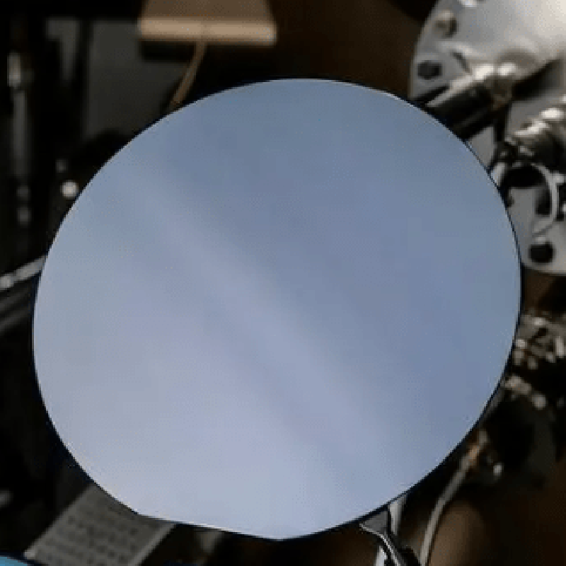
One of the key areas in which Quartz Tube has made significant strides is in the field of semiconductor manufacturing. The company’s quartz tubes are widely used in the production of semiconductors, where the purity and quality of the material are crucial for ensuring the performance and reliability of the final products. Quartz Tube’s products have set new benchmarks for purity and consistency, making them the go-to choice for semiconductor manufacturers around the world.
In addition to semiconductor manufacturing, Quartz Tube’s products have also found extensive applications in the field of solar technology. The company’s quartz tubes are used in the production of high-quality quartz glass crucibles, which are essential for the melting and refining of silicon for solar cells. The exceptional thermal and chemical properties of Quartz Tube’s products make them ideal for this critical stage of solar panel production, enabling manufacturers to achieve the high levels of purity and efficiency required for top-tier solar panels.
Furthermore, Quartz Tube has been a key player in the development of advanced lighting systems. The company’s quartz tubes are utilized in the production of high-performance quartz-glass products that are essential for cutting-edge lighting solutions, including halogen lamps, mercury vapor lamps, and UV lamps. The exceptional clarity, heat resistance, and thermal stability of Quartz Tube’s products make them the preferred choice for manufacturers looking to create innovative lighting solutions that meet the high standards of modern technology and design.
Beyond these specific applications, Quartz Tube’s products have also found use in a wide range of other industries, including chemical processing, medical equipment, and telecommunications. The company’s dedication to quality and innovation has earned it a strong reputation for providing reliable and high-performance quartz tubing solutions that meet the diverse needs of its global customer base.
At the heart of Quartz Tube’s success is its unwavering commitment to research and development. The company invests heavily in exploring new technologies and materials, as well as in improving its manufacturing processes to maintain its position as a leader in the field of quartz tubing. By collaborating with leading experts and institutions in materials science and engineering, Quartz Tube continues to push the boundaries of what is possible with quartz, driving innovation and shaping the future of various industries.
Looking ahead, Quartz Tube is set to continue its trajectory of success and growth, with a strong pipeline of new products and collaborations on the horizon. The company’s relentless pursuit of excellence and its dedication to meeting the evolving needs of its customers make it well-positioned to remain a driving force in the world of quartz tubing for years to come.
In conclusion, Quartz Tube has firmly established itself as a trailblazer in the field of quartz tubing, with a track record of delivering innovative solutions that have transformed industries around the world. With its cutting-edge products and unwavering commitment to research and development, the company is well-positioned to continue shaping the future of various high-tech industries for years to come. As the demand for high-quality quartz tubing continues to grow, Quartz Tube is poised to play a pivotal role in driving the next wave of technological innovation and progress.
Company News & Blog
High-quality Sapphire Wafer for A-Plane Axis Applications
A-plane Axis, a cutting-edge technology company, recently announced the launch of their revolutionary sapphire wafer for use in the aerospace industry. This breakthrough product promises to revolutionize the way planes are designed and built, by providing a more durable and reliable material for use in critical components.The A-plane Axis sapphire wafer is made from high-purity synthetic sapphire, a material known for its exceptional hardness and resistance to wear and corrosion. This makes it ideal for use in aerospace applications, where components are subjected to extreme conditions and must withstand high levels of stress and wear.The unique properties of sapphire make it an excellent choice for use in critical components such as bearings, seals, and other parts that are subjected to high levels of friction and wear. Its exceptional hardness and wear resistance make it far superior to traditional materials such as metal alloys or ceramics, which are more prone to wear and degradation over time.In addition to its exceptional durability, the A-plane Axis sapphire wafer also offers other key advantages for aerospace applications. Its high thermal conductivity and excellent electrical insulation properties make it well-suited for use in high-temperature and high-voltage applications, where traditional materials may struggle to perform.Furthermore, the use of sapphire in aerospace components can also lead to significant weight savings, as it is a lightweight material compared to traditional metal alloys. This can contribute to overall fuel efficiency and reduce the environmental impact of aircraft operations, a key consideration for the aviation industry.The launch of the A-plane Axis sapphire wafer represents a major milestone for the company, which has positioned itself as a leader in advanced materials technology for aerospace applications. With a strong focus on research and development, A-plane Axis has invested heavily in the development of new and innovative materials to meet the evolving needs of the aerospace industry.The company's state-of-the-art manufacturing facilities and cutting-edge production techniques enable them to produce sapphire wafers with exceptional precision and consistency, ensuring that they meet the stringent quality standards required for aerospace applications.A-plane Axis's sapphire wafer is already gaining attention from leading aerospace manufacturers, who are keen to take advantage of its unique properties to improve the performance and reliability of their aircraft. With the potential to enhance the durability, efficiency, and safety of aerospace components, the use of sapphire wafers could have a transformative impact on the industry as a whole.In addition to aerospace applications, A-plane Axis is also exploring the potential use of sapphire wafers in other industries, such as semiconductor manufacturing, automotive, and medical devices. The versatility and unique properties of sapphire make it a promising material for a wide range of applications, and the company is committed to exploring new opportunities for its use.As the aerospace industry continues to evolve and demand for more advanced materials grows, A-plane Axis is well-positioned to be at the forefront of this technological revolution. With its innovative sapphire wafer, the company is poised to make a lasting impact on the way aircraft are designed and built, leading to safer, more efficient, and more reliable air travel for years to come.
High-quality Science Lab Equipment for All Your Research Needs
Science Lab Equipment Introduces Latest Technology for Research and EducationScience Lab Equipment, a leading provider of laboratory equipment and supplies, has recently introduced their latest range of cutting-edge technology for research and education. With a strong focus on innovation and quality, the company has made significant advancements in the field of laboratory equipment, catering to the needs of both scientific research and educational institutions.The new range of products includes state-of-the-art laboratory instruments, tools, and supplies, designed to meet the evolving needs of modern research and educational environments. From basic laboratory essentials to advanced scientific instruments, Science Lab Equipment offers a comprehensive range of solutions for various scientific disciplines, including biology, chemistry, physics, and environmental science.With a commitment to excellence, Science Lab Equipment has partnered with leading manufacturers and suppliers to bring the latest advancements in laboratory technology to their customers. By continuously updating their product range, the company ensures that researchers, scientists, and educators have access to the most advanced and reliable equipment for their work.One of the key highlights of Science Lab Equipment's latest range is the introduction of advanced instrumentation for molecular biology research. This includes state-of-the-art PCR machines, DNA sequencers, and gel electrophoresis systems, which are essential for exploring the complexities of genetics and biochemistry. These cutting-edge technologies are expected to revolutionize the way researchers conduct experiments and analyze biological processes.In addition to their focus on research, Science Lab Equipment also caters to the needs of educational institutions, providing a wide range of laboratory supplies for teaching and learning purposes. From basic glassware and safety equipment to advanced scientific models and demonstration kits, the company offers a comprehensive range of resources for educators to enhance their teaching methodologies and engage students in hands-on learning experiences.Furthermore, Science Lab Equipment emphasizes the importance of quality and reliability in all of their products. Through rigorous testing and quality control measures, the company ensures that their equipment meets the highest standards of performance and safety. This commitment to quality has earned Science Lab Equipment a strong reputation among their customers, who value the reliability and durability of their products.Moreover, in response to the growing demand for sustainable solutions, Science Lab Equipment has also expanded their range of environmentally-friendly laboratory supplies. This includes eco-friendly consumables, energy-efficient instruments, and recyclable materials, reflecting the company's dedication to promoting sustainable practices in scientific research and education.With their extensive product range, commitment to quality, and focus on innovation, Science Lab Equipment remains at the forefront of the laboratory equipment industry. Their dedication to meeting the evolving needs of researchers and educators has positioned them as a trusted provider of cutting-edge technology for scientific exploration and learning. By partnering with leading manufacturers and suppliers, the company continues to bring the latest advancements in laboratory technology to their customers, ensuring that scientists and educators have access to the most advanced and reliable equipment for their work.In conclusion, Science Lab Equipment's latest range of products represents a significant leap forward in the field of laboratory technology. With a strong emphasis on innovation, quality, and sustainability, the company remains committed to providing researchers and educators with the most advanced tools and resources for their work. As the demand for advanced laboratory technology continues to grow, Science Lab Equipment stands ready to meet the needs of the scientific and educational communities with their state-of-the-art solutions.
Gallium Arsenide: A Revolutionary New Material Taking the Semiconductor Industry by Storm
Galliumarsenide (GaAs) , a compound of gallium and arsenic, has emerged as a crucial material in the development of semiconductors and other electronic devices. The unique properties of GaAs have made it an attractive choice for a wide range of applications, from mobile phone components to solar cells. As the demand for more efficient and powerful electronic devices continues to grow, GaAs has become increasingly important in the technology industry.{} is at the forefront of the use of GaAs in electronic devices. With a strong focus on research and development, {} has been able to harness the unique properties of GaAs to create innovative and high-performance products. The company has a long history of expertise in semiconductor materials, and has proven itself as a leader in the use of GaAs in electronic devices.One of the key advantages of GaAs is its high electron mobility, which allows for the creation of faster and more efficient electronic devices. This has made GaAs an ideal material for high-frequency applications, such as mobile phone components and radio-frequency (RF) devices. In addition, GaAs has a direct bandgap, which allows for the efficient generation and detection of light. This property has made GaAs a popular choice for optoelectronic devices, such as solar cells and light-emitting diodes (LEDs).{} has been able to leverage these properties of GaAs to create a range of cutting-edge electronic devices. The company's GaAs-based products have been widely adopted in the telecommunications industry, where high-frequency and high-speed devices are essential for the transmission of data. In addition, {} has developed a strong presence in the optoelectronics market, with GaAs-based solar cells and LEDs that offer high efficiency and long lifetimes.In recent years, {} has also made significant strides in the development of GaAs-based power devices. These devices are capable of handling high voltages and currents, and are crucial for a range of applications, from power electronics to electric vehicles. {}'s GaAs-based power devices have been well-received in the market, with their high efficiency and reliability making them a preferred choice for a wide range of applications.One of the key strengths of {} is its commitment to research and development. The company has a dedicated team of scientists and engineers who are constantly pushing the boundaries of what is possible with GaAs. By continually exploring new applications and technologies, {} has been able to stay ahead of the curve in the rapidly evolving semiconductor industry.In addition to its technical expertise, {} has also established strong partnerships with leading companies in the semiconductor and electronics industries. This has allowed the company to access the latest technologies and manufacturing processes, ensuring that its GaAs-based products are of the highest quality and performance.Looking to the future, {} is continuing to invest in the development of GaAs-based electronic devices. The company is exploring new applications for GaAs, and is working to further improve the efficiency and performance of its products. With its strong technical expertise and dedication to innovation, {} is well-positioned to remain a leader in the use of GaAs in electronic devices.In conclusion, Galliumarsenide (GaAs) has emerged as a crucial material in the development of high-performance electronic devices. {} has been at the forefront of the use of GaAs in electronic devices, leveraging the unique properties of this material to create innovative and cutting-edge products. With its strong focus on research and development, technical expertise, and commitment to innovation, {} is well-positioned to continue leading the way in the use of GaAs in electronic devices.
Advanced Crystal Ingot Technologies Discovered for Enhanced Laser Applications
**Title: Groundbreaking YAG Crystal Ingot Revolutionizes the Semiconductor Industry***Date: [Insert Date]**Location: [Insert Location]**Introduction*In a groundbreaking development, a revolutionary YAG Crystal Ingot has emerged on the market, transforming the semiconductor industry. This high-performance crystal ingot, developed by [Company Name], promises to elevate the efficiency and functionality of electronic devices to unprecedented levels. With its exceptional properties, the YAG Crystal Ingot is poised to revolutionize various sectors, including telecommunications, consumer electronics, and even medicine.*Company Overview*[Company Name], a leading innovator in the field of advanced materials, has established itself as a pioneer in developing cutting-edge technologies. Focused on pushing the boundaries of what is possible, the company has constantly strived to develop solutions that address the evolving needs of industries globally. Their relentless pursuit of excellence has earned them a prominent position, with their products being used extensively across various sectors.*YAG Crystal Ingot: The Game Changer*The YAG Crystal Ingot, developed by [Company Name]'s team of brilliant scientists and engineers, has created a buzz in the semiconductor manufacturing domain. This crystal ingot is made from yttrium aluminum garnet, or YAG, which exhibits exceptional optical and thermal properties. The unique combination of these properties enables the YAG Crystal Ingot to outperform existing semiconductor materials in several key aspects.One of the most significant advantages of the YAG Crystal Ingot is its outstanding thermal conductivity. High thermal conductivity is essential in semiconductor applications, as it aids in efficiently dissipating heat generated during device operation. The YAG Crystal Ingot, thanks to its superior thermal conductivity, ensures that electronic devices can operate at higher power levels without the risk of overheating, ultimately boosting their performance and longevity.Additionally, the YAG Crystal Ingot's optical properties allow for enhanced light transmission, making it perfect for applications in optoelectronic devices such as lasers, LEDs, and optical amplifiers. Its ability to efficiently transmit light across a broad spectrum enables manufacturers to create more efficient and reliable devices, benefiting industries such as telecommunications, data centers, and medical diagnostics.Moreover, the YAG Crystal Ingot exhibits exceptional mechanical properties, offering superior resistance to shocks and vibrations. This resilience makes it an ideal material for manufacturing devices meant for rugged environments or those subjected to constant movement, such as aerospace and defense equipment.The outstanding performance of the YAG Crystal Ingot is a testament to [Company Name]'s commitment to advancing technology and delivering innovative solutions. Their investment in research and development has allowed them to overcome the limitations of traditional materials and introduce a game-changing semiconductor product.*Envisioning the Future*The implications of the YAG Crystal Ingot's development are profound and far-reaching. Industries that rely heavily on semiconductor technology, such as telecommunications, consumer electronics, automotive, and healthcare, will experience a paradigm shift with the integration of this advanced material.Telecommunications companies will benefit from the YAG Crystal Ingot's ability to enhance the overall efficiency and reliability of their networks. Faster data transfer, lower latency, and improved signal quality will improve the end-user experience and lay the groundwork for the future of connectivity.Consumer electronics will witness a new era of technological advancements, with devices that exhibit higher performance, improved energy efficiency, and longer lifespans. From smartphones to smart home devices, the integration of YAG Crystal Ingot will elevate the functionality and durability of these products, delighting consumers across the globe.The medical field will also embrace the YAG Crystal Ingot, as it offers groundbreaking opportunities for better diagnostic tools, advanced surgical equipment, and the development of innovative health monitoring devices. Improved precision, reliability, and safety will revolutionize patient care and enable medical professionals to achieve groundbreaking breakthroughs.*Conclusion*With the introduction of the YAG Crystal Ingot, [Company Name] has truly changed the game in the semiconductor industry. This remarkable crystal ingot's superior thermal conductivity, optical properties, and mechanical resilience make it an invaluable material for various applications. By leveraging the potential of the YAG Crystal Ingot, industries can elevate their performance, redefine technological norms, and ultimately shape a future that is brighter, faster, and more efficient than ever before.
Lithium Niobate Thin Film: Advancements in Thin Film Technology
Lithium Niobate Thin Film: Revolutionizing the World of ElectronicsIn today's rapidly growing technology-driven world, the demand for smaller, faster, and more efficient electronic devices is higher than ever. To meet this ever-increasing demand, {company name} has recently developed a breakthrough technology in the form of Lithium Niobate Thin Film. This cutting-edge innovation is set to revolutionize the world of electronics and pave the way for the development of next-generation electronic devices.Lithium Niobate Thin Film is a key component in the manufacture of various electronic devices, such as mobile phones, computers, and high-speed data communication systems. The unique properties of this thin film, such as its high refractive index, excellent piezoelectric and electro-optic properties, and wide transparency range, make it an ideal material for use in the production of advanced electronic devices.{company name} is a leading global technology company that specializes in the research, development, and production of advanced materials for a wide range of industries, including electronics, telecommunications, and renewable energy. With a strong focus on innovation and sustainability, the company is committed to creating cutting-edge solutions that address the evolving needs of the modern world.The development of Lithium Niobate Thin Film is a result of {company name}'s relentless dedication to research and development. By leveraging its expertise in material science and engineering, the company has succeeded in creating a thin film that not only meets the current market demands but also sets new standards for performance and reliability.One of the key advantages of Lithium Niobate Thin Film is its ability to significantly enhance the performance of electronic devices. Its high refractive index allows for the fabrication of miniature optical components, which play a crucial role in the development of compact and high-speed communication systems. This, in turn, enables the creation of smaller and more energy-efficient electronic devices, which are essential for meeting the growing demands of modern consumers.Furthermore, the exceptional piezoelectric and electro-optic properties of Lithium Niobate Thin Film make it an ideal material for use in the production of advanced sensors and actuators. These sensors and actuators have a wide range of applications, including medical devices, automotive systems, and industrial machinery, where accuracy, reliability, and responsiveness are essential.In addition to its superior performance characteristics, Lithium Niobate Thin Film also offers a wide transparency range, making it suitable for use in the development of high-definition displays and imaging systems. This opens up new opportunities for the creation of advanced electronic devices with enhanced visual quality and clarity, catering to the needs of industries such as entertainment, healthcare, and education.As the demand for smaller, faster, and more efficient electronic devices continues to grow, the development of advanced materials such as Lithium Niobate Thin Film becomes increasingly crucial. It is evident that {company name} is at the forefront of this technological revolution, driving innovation and shaping the future of the electronics industry.With its proven track record of delivering cutting-edge solutions, combined with its unwavering commitment to sustainability and social responsibility, {company name} is well-positioned to lead the way in the development and production of advanced materials for the electronics industry. The introduction of Lithium Niobate Thin Film further solidifies the company's position as a key player in the global technology market.In conclusion, the development of Lithium Niobate Thin Film by {company name} represents a significant leap forward in the world of electronics. This breakthrough innovation is set to redefine the performance and capabilities of electronic devices, opening up new possibilities for the creation of smaller, faster, and more efficient products. As the demand for advanced electronic devices continues to rise, the introduction of Lithium Niobate Thin Film is a testament to {company name}'s commitment to driving innovation and shaping the future of technology.
Get the Latest Updates on 300mm Wafer Technology in the News
The semiconductor industry is seeing a major shift with the increasing demand for advanced technology in various sectors such as automotive, healthcare, and consumer electronics. To meet this growing demand, the need for high-quality and efficient wafer manufacturing has become crucial. With this in mind, a prominent company in the semiconductor industry, {} has recently announced the introduction of their state-of-the-art 300mm wafer technology.{}has been at the forefront of semiconductor manufacturing, known for its cutting-edge solutions and innovative products. The company has a strong focus on research and development, consistently striving to push the boundaries of semiconductor technology. With the introduction of the 300mm wafer, the company aims to further solidify its position in the industry and cater to the evolving needs of its customers.The 300mm wafer technology has several advantages over the traditional 200mm wafer, including increased production capacity and improved efficiency. With a larger surface area, the 300mm wafer allows for more chips to be fabricated in a single production cycle, leading to higher yields and reduced manufacturing costs. This is particularly beneficial in meeting the high-volume demands of modern semiconductor applications.In addition to the increased production capacity, the 300mm wafer also offers enhanced performance and reliability. The larger size allows for better thermal management and reduced power consumption, making it ideal for high-performance applications such as data centers, artificial intelligence, and 5G technology. Moreover, the company's advanced fabrication processes ensure the highest level of quality and precision, meeting the stringent requirements of the industry.The introduction of the 300mm wafer is a testament to {}'s commitment to driving innovation and shaping the future of semiconductor technology. With its extensive expertise and cutting-edge manufacturing capabilities, the company is well-positioned to lead the industry in the transition to larger wafer sizes. This move not only demonstrates the company's technical prowess but also its dedication to meeting the evolving needs of its customers.Furthermore, {}'s 300mm wafer technology is poised to have a significant impact on the semiconductor industry as a whole. The increased production capacity and efficiency will enable semiconductor manufacturers to keep pace with the growing demand for advanced technology across various sectors. This is particularly crucial as industries such as automotive and healthcare increasingly rely on semiconductor solutions for their products and services.The introduction of the 300mm wafer technology also aligns with the industry's overall trend towards larger wafer sizes. As the demand for semiconductor devices continues to rise, larger wafers are seen as a key enabler for meeting this demand in a cost-effective and efficient manner. {}'s investment in this advanced technology reaffirms its position as a key player in driving this transition and shaping the future of semiconductor manufacturing.With the introduction of the 300mm wafer technology, {} is not only enhancing its own capabilities but also contributing to the overall advancement of the semiconductor industry. By providing high-quality, high-performance wafers, the company is enabling its customers to develop cutting-edge semiconductor solutions that will power the technologies of tomorrow. This is a testament to {}'s ongoing dedication to innovation and its commitment to delivering value to its customers and the industry as a whole.In conclusion, the introduction of the 300mm wafer technology by {} marks a significant milestone in the semiconductor industry. With its advanced capabilities and potential to drive efficiency and innovation, this move is set to have a major impact on the industry as a whole. As the demand for advanced semiconductor solutions continues to grow, {} is well-positioned to lead the way with its state-of-the-art wafer manufacturing technology.
New Airplane Technology Revolutionizes Travel Industry
Sapphire Plane, a groundbreaking aircraft, is set to revolutionize the aviation industry with its cutting-edge technology and sleek design. Developed by a team of experts at {company name}, this aircraft promises to deliver unparalleled performance, efficiency, and comfort for both passengers and crew. With its innovative features and state-of-the-art systems, Sapphire Plane is poised to set new standards in the world of air travel.The aircraft's development is the result of years of research and development by {company name}, a leading aerospace company known for its commitment to excellence and innovation. With a track record of delivering top-of-the-line aircraft and aerospace products, {company name} has established itself as a driving force in the industry. The development of Sapphire Plane is a testament to the company's dedication to pushing the boundaries of what is possible in aviation.One of the key highlights of Sapphire Plane is its advanced propulsion system, which is designed to deliver superior fuel efficiency and reduced environmental impact. This cutting-edge technology not only makes the aircraft more cost-effective to operate but also aligns with the global push towards sustainability in aviation. With a focus on reducing carbon emissions and minimizing environmental footprint, Sapphire Plane is set to be a game-changer in the quest for greener air travel.In addition to its state-of-the-art propulsion system, Sapphire Plane boasts a sleek and modern design that prioritizes passenger comfort and convenience. The spacious cabin is equipped with luxurious amenities and advanced entertainment systems, ensuring that passengers have a pleasant and enjoyable flight experience. The aircraft's ergonomically designed seats and customizable interior options further enhance the overall comfort for travelers, making it an attractive choice for discerning passengers.Furthermore, Sapphire Plane is equipped with the latest in avionics and safety technologies, providing a secure and reliable flying experience. With advanced navigation systems, redundant safety features, and real-time monitoring capabilities, the aircraft offers peace of mind for both passengers and crew. The commitment to safety and reliability is a priority for {company name}, and Sapphire Plane is a testament to the company's dedication to providing the highest standards of aircraft technology and design.Moreover, Sapphire Plane is designed with the operational efficiency of airlines in mind, offering a range of features that optimize flight operations and maintenance. The aircraft's advanced systems and components are engineered to minimize downtime and reduce long-term operating costs, making it an attractive option for airlines seeking to improve their bottom line without compromising on quality and performance.The launch of Sapphire Plane represents a significant milestone for {company name}, as it solidifies the company's position as a leader in the development of cutting-edge aerospace technology. With its innovative design, state-of-the-art features, and unwavering commitment to excellence, Sapphire Plane is set to make a lasting impact in the aviation industry.In conclusion, the development of Sapphire Plane by {company name} signals a new era in aviation, one that prioritizes efficiency, performance, and sustainability. With its advanced technology and luxurious design, the aircraft is poised to set new standards for air travel, redefining the flying experience for passengers and crew alike. {company name}'s dedication to excellence and innovation is clearly reflected in the development of Sapphire Plane, and the aircraft is set to make a lasting impact in the aviation industry for years to come.
High Resistivity Silicon Wafer: A Breakthrough Innovation in Semiconductor Technology
[Headline]High Resistivity Silicon Wafer: Revolutionizing Semiconductor Applications[Date][City], [State] - [Company Name], a leading provider of innovative semiconductor solutions, introduces its highly anticipated High Resistivity Silicon Wafer, marking a significant advancement in the semiconductor industry. This revolutionary new product is poised to reshape various technology sectors by offering superior performance and enhanced conductivity in semiconductor applications.[City], [State] – [Company Name], a trailblazer in the semiconductor industry, has unveiled its latest groundbreaking product – the state-of-the-art High Resistivity Silicon Wafer. This cutting-edge innovation promises to redefine the standards of precision and efficiency in semiconductor applications, opening new avenues for technological advancements across multiple sectors.The High Resistivity Silicon Wafer is designed to address the growing demand for improved conductivity, reduced resistance, and enhanced performance in semiconductor devices. This advanced development enables better control over electrical characteristics, making it particularly useful in applications such as power electronics, microwave devices, and radiation detectors.With its revolutionary properties and exceptional material quality, the High Resistivity Silicon Wafer significantly outperforms its competitors. The wafer boasts an impressively high resistivity level, enabling better isolation between devices, resulting in minimized crosstalk and reduced power consumption. Semiconductor manufacturers can now achieve greater levels of integration density and performance in their products.One of the key advantages of the High Resistivity Silicon Wafer lies in its superior frequency response, making it an ideal choice for advanced microwave devices. The wafer’s low parasitic capacitance and improved signal-to-noise ratio lead to enhanced sensitivity and precision in high-frequency applications such as Wi-Fi, radio frequency identification (RFID), and satellite communications.Moreover, the High Resistivity Silicon Wafer offers exceptional performance in power electronics. Its unique material composition ensures better control of leakage currents, allowing for increased efficiency and reduced power wastage in devices such as power diodes and thyristors. With the ability to handle higher voltages and temperatures, the wafer can support advanced power management systems, renewable energy technologies, and electric vehicle charging infrastructure.In addition to power electronics and microwave devices, the High Resistivity Silicon Wafer can be employed in radiation detectors. Its increased resistivity allows for the precise detection of radiation, making it an indispensable component in medical imaging equipment, nuclear power plants, and space exploration instrumentation.As the demand for more advanced semiconductor devices rapidly grows, [Company Name] remains at the forefront of innovation by developing groundbreaking solutions. The company's extensive expertise in semiconductor manufacturing, coupled with its state-of-the-art facilities, enables the production of high-quality and reliable semiconductor wafers that meet the most stringent industry standards.[Company Name] is dedicated to creating value for its customers by delivering cutting-edge semiconductor solutions. The company's commitment to research and development ensures that it stays ahead of the competition, constantly adapting to the evolving needs of the industry. With the launch of the High Resistivity Silicon Wafer, [Company Name] adds another valuable addition to its portfolio of innovative products.The introduction of the High Resistivity Silicon Wafer marks a milestone moment in the semiconductor industry. This revolutionary product showcases the pioneering spirit of [Company Name] and its determination to push the boundaries of technological possibilities. With its exceptional conductivity, improved device performance, and unparalleled material quality, the High Resistivity Silicon Wafer will undoubtedly revolutionize semiconductor applications across various sectors, driving progress and innovation for years to come.
Semiconductor Breakthrough: New Gallium Compound Shows Promise for Advancing Technology
Gallium Semiconductor (brand name removed), a leading player in the semiconductor industry, recently made headlines with their innovative solutions that are set to revolutionize various electronics and technology sectors. The company has been at the forefront of developing advanced semiconductor technologies and has been consistently pushing the boundaries of what is possible in the world of electronics.Gallium Semiconductor is known for its cutting-edge research and development in the field of semiconductor materials and devices. The company has a team of world-class engineers and scientists who are constantly working on developing new and improved semiconductor solutions that can meet the ever-evolving demands of the electronics industry.One of the key areas where Gallium Semiconductor has made significant strides is in the development of gallium-based semiconductor materials. Gallium-based semiconductors have unique properties that make them highly desirable for a wide range of applications. These materials offer higher electron mobility and power efficiency, making them ideal for use in high-performance electronics, including 5G devices, high-speed data processing, and power electronics.In addition to their work on gallium-based materials, Gallium Semiconductor has also been actively involved in the development of advanced semiconductor devices. The company has been working on next-generation transistors, diodes, and other semiconductor components that offer improved performance and energy efficiency. These advancements have the potential to drive significant improvements in electronics, enabling faster and more powerful devices across various industries.Furthermore, Gallium Semiconductor has been making significant investments in the development of wide-bandgap semiconductors. Wide-bandgap materials such as silicon carbide and gallium nitride offer superior performance compared to traditional silicon-based semiconductors. These materials can operate at higher temperatures, frequencies, and voltages, making them well-suited for use in power electronics and automotive applications.Gallium Semiconductor's commitment to innovation and excellence has garnered the attention of industry leaders and partners. The company has been actively collaborating with other technology firms, research institutions, and government agencies to further advance semiconductor technologies and bring cutting-edge solutions to the market.One of the notable partnerships that Gallium Semiconductor has formed is with leading electronics manufacturers to integrate their semiconductor solutions into a wide range of consumer products. This collaboration aims to bring the latest semiconductor advancements to everyday devices, such as smartphones, laptops, and smart appliances, enhancing their performance and energy efficiency.In addition to their work with consumer electronics, Gallium Semiconductor has also been focusing on the automotive industry. The company's advanced semiconductor solutions have the potential to drive innovation in electric and autonomous vehicles, enabling greater efficiency and performance in the next generation of automobiles.The impact of Gallium Semiconductor's advancements in the semiconductor industry is expected to be far-reaching. Their innovative solutions have the potential to drive significant improvements in a wide range of electronic devices and systems, from mobile devices and computers to renewable energy systems and electric vehicles.Gallium Semiconductor has demonstrated a strong commitment to sustainability and environmental responsibility. The company's semiconductor materials and devices offer energy-efficient solutions that can contribute to reducing the overall carbon footprint of electronic devices and systems.As the demand for high-performance electronics continues to grow, Gallium Semiconductor is well-positioned to lead the way in driving innovation and shaping the future of the semiconductor industry. With their focus on advanced materials and devices, the company is poised to play a pivotal role in accelerating the development of next-generation electronics and technology solutions.In conclusion, Gallium Semiconductor's dedication to innovation and excellence has positioned them as a key player in the semiconductor industry. Their groundbreaking advancements in semiconductor materials and devices are expected to have a transformative impact on various electronics and technology sectors, driving significant improvements in performance, energy efficiency, and sustainability. As the demand for high-performance electronics continues to rise, Gallium Semiconductor is set to play a pivotal role in shaping the future of the semiconductor industry and driving innovation across a wide range of applications.
Chemical Mechanical Polishing: The Latest Advancements and Applications
Cmp Chemical Mechanical Polishing (CMP) has quickly become a leading provider of advanced surface polishing solutions for the semiconductor and microelectronics industries. The company's innovative and high-performance products have positioned them as a trusted partner for leading integrated device manufacturers (IDMs), foundries, and equipment suppliers. With an ever-increasing demand for high-quality and high-precision polishing processes, CMP is carving out a strong presence in the global market.Since its inception, CMP has been dedicated to delivering cutting-edge solutions that meet the evolving needs of the industry. The company's comprehensive portfolio includes a wide range of products and services, including polishing slurries, pads, and polishing tools. These solutions are designed to enable customers to achieve the highest levels of performance, productivity, and cost-effectiveness in their manufacturing processes.CMP's success can be attributed to its commitment to continuous innovation and a customer-centric approach. The company's team of experts possess a deep understanding of the complex requirements of the semiconductor industry, enabling them to develop tailor-made solutions for individual customer needs. By leveraging advanced technologies and state-of-the-art facilities, CMP is able to deliver products that meet the highest industry standards while also providing a competitive edge for its customers.One of CMP's key strengths lies in its ability to provide comprehensive technical support and customer service. The company's dedicated technical team works closely with customers to understand their specific requirements and challenges, offering expert guidance and troubleshooting assistance throughout the entire process. This level of support ensures that customers are able to fully maximize the capabilities of CMP's products and achieve their desired outcomes.Furthermore, CMP's commitment to sustainability and environmental responsibility sets it apart from its competitors. The company prioritizes the development of environmentally-friendly products and processes, aiming to minimize the environmental impact of its operations. By investing in research and development of green technologies, CMP is not only helping its customers meet their sustainability goals but also contributing to the overall advancement of the industry.CMP's strong reputation for quality, reliability, and innovation has positioned it as a trusted partner for the world's leading semiconductor and microelectronics companies. The company's solutions have been instrumental in enabling customers to optimize their manufacturing processes, improve yields, and reduce costs. As the demand for high-performance polishing solutions continues to grow, CMP is well-positioned to capitalize on new opportunities and expand its global footprint.Looking ahead, CMP is focused on driving further advancements in surface polishing technology and embracing new opportunities for growth. The company remains committed to its core values of innovation, customer satisfaction, and sustainability, cementing its position as a leader in the industry.In conclusion, CMP Chemical Mechanical Polishing has emerged as a key player in the semiconductor and microelectronics industries, providing cutting-edge surface polishing solutions that enable customers to achieve superior performance, efficiency, and sustainability. With a relentless focus on innovation and customer satisfaction, CMP is poised to continue its upward trajectory and solidify its position as a top-tier provider of advanced polishing technologies.