
High-quality Gallium Arsenide Wafer for Electronic Applications
By:Admin
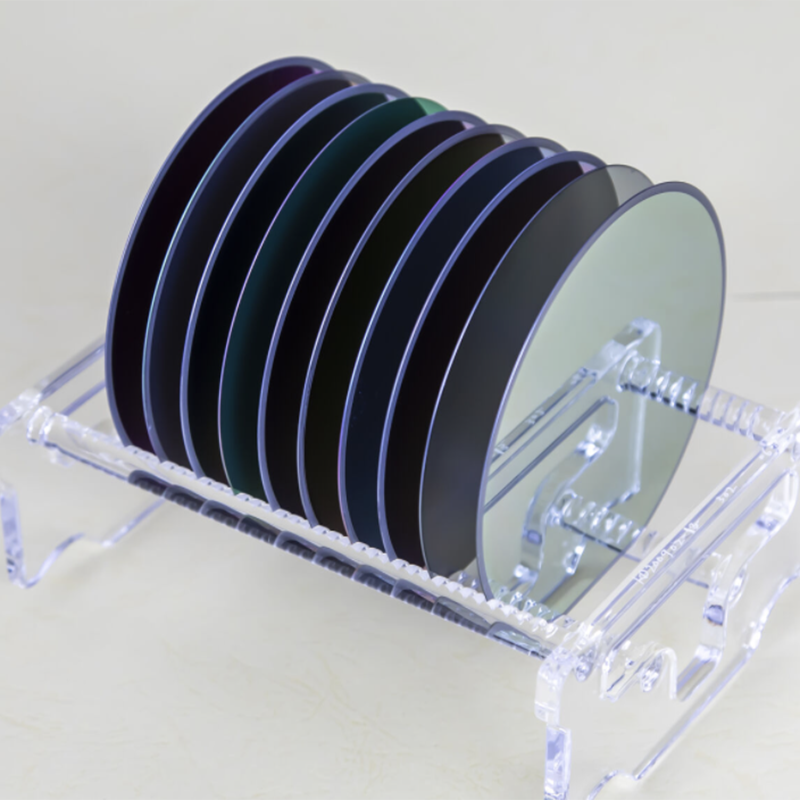
Gallium Arsenide wafers are semiconductor materials that have several advantages over traditional silicon wafers. They offer higher electron mobility, which results in faster electronic devices, and they can operate at higher temperatures, making them ideal for high-power applications. Additionally, Gallium Arsenide has a direct bandgap, which allows it to emit light more efficiently than silicon. This makes it a perfect material for optoelectronic devices such as LEDs and solar cells.
The company has perfected the manufacturing process for Gallium Arsenide wafers, ensuring that they meet the highest quality standards. Their wafers are available in various sizes and thicknesses, making them suitable for a wide range of applications. Whether it's for advanced wireless communication systems, high-speed data transfer, or satellite technology, these wafers are poised to enable the next generation of electronic devices.
One of the most exciting potential applications for Gallium Arsenide wafers is in the development of 5G technology. With the demand for faster and more reliable wireless communication growing rapidly, 5G networks are set to revolutionize the way we connect and communicate. Gallium Arsenide wafers can enable the high-frequency operation required for 5G devices, making them an essential component in the rollout of this next-generation technology.
In addition to telecommunications, Gallium Arsenide wafers have the potential to drive advancements in aerospace and defense. The superior performance of these wafers makes them ideal for radar and communication systems used in military and aerospace applications. Their ability to operate at higher frequencies and temperatures makes them a key enabler for sophisticated electronic systems in these critical fields.
The company's commitment to research and development has positioned them as a leader in Gallium Arsenide technology. They continue to invest in refining their manufacturing processes and expanding their product offerings to meet the evolving needs of the semiconductor industry. Their team of experienced engineers and scientists are dedicated to pushing the boundaries of what is possible with Gallium Arsenide, driving innovation and shaping the future of electronic devices.
As the demand for faster, more efficient electronic devices continues to grow, the importance of advanced semiconductor materials like Gallium Arsenide cannot be overstated. The unique properties of this material make it a key enabler for the development of cutting-edge technologies in various industries. With their expertise and commitment to excellence, the company is well-positioned to drive the widespread adoption of Gallium Arsenide wafers and shape the future of semiconductor technology.
Company News & Blog
High Quality Double Side Polished Silicon Wafers for Sale
Double Side Polished Silicon Wafers: The Latest Innovation from Leading Technology CompanySilicon wafers are an essential component in the production of semiconductor devices, and the demand for high-quality wafers continues to grow as the technology industry expands. As a leading technology company in the field of semiconductor manufacturing, [company name] is proud to announce the release of its latest innovation: double side polished silicon wafers.Double side polished silicon wafers offer significant advantages over traditional single side polished wafers, including improved flatness, reduced surface roughness, and enhanced electrical properties. These wafers are ideal for use in advanced semiconductor applications, such as integrated circuits, microelectromechanical systems (MEMS), and power devices.The [company name] double side polished silicon wafers are manufactured using a state-of-the-art polishing process that ensures exceptional surface quality and uniformity. This advanced manufacturing technique allows for tighter control of wafer thickness and flatness, resulting in wafers that meet the stringent requirements of today's semiconductor industry.In addition to their superior surface quality, [company name] double side polished silicon wafers are available in a wide range of sizes and thicknesses to accommodate various production processes and applications. Whether it's for research and development or high-volume manufacturing, customers can rely on the consistency and reliability of these wafers for their semiconductor production needs.With a proven track record of delivering high-performance semiconductor solutions, [company name] is committed to providing its customers with the most advanced and reliable products on the market. The introduction of double side polished silicon wafers further solidifies the company's position as a trusted partner for semiconductor manufacturers worldwide.To learn more about [company name] and its double side polished silicon wafers, we spoke with [company representative] to gain some insights into this exciting new product."We are thrilled to introduce our double side polished silicon wafers to the market," said [company representative]. "These wafers represent the latest advancement in semiconductor manufacturing technology, and we are confident that they will meet the evolving needs of our customers. Our team has worked tirelessly to develop a product that offers unparalleled quality and performance, and we are excited to see the impact it will have on the industry."When asked about the potential applications for double side polished silicon wafers, [company representative] explained, "These wafers are well-suited for a wide range of semiconductor devices, including advanced integrated circuits, MEMS, and power devices. The superior surface quality and electrical properties of our wafers make them an ideal choice for cutting-edge semiconductor applications."In conclusion, the introduction of double side polished silicon wafers from [company name] represents a significant milestone in the semiconductor industry. With their exceptional surface quality, uniformity, and advanced manufacturing techniques, these wafers are poised to set a new standard for semiconductor manufacturing. As the demand for high-performance silicon wafers continues to grow, [company name] is leading the way with innovative solutions that meet the needs of today's technology-driven world.
High-Quality Single Crystal Silicon Wafers: The Latest in Semiconductor Technology
Single Crystal Silicon Wafer Technology Advancements Revolutionize Semiconductor IndustryWith the continued demand for smaller and more powerful electronic devices, the semiconductor industry has been continuously striving to innovate and improve the technology that drives these devices. One company at the forefront of this innovation is [Company Name], a leading manufacturer of single crystal silicon wafers.[Company Name] specializes in the production of high-quality single crystal silicon wafers that are used in the manufacturing of semiconductors and electronic devices. These wafers serve as the foundation for the production of integrated circuits that power a wide range of applications, including smartphones, computers, automotive electronics, and more.The company's dedication to research and development has led to significant advancements in single crystal silicon wafer technology, making it possible to produce wafers with superior quality and performance. Their state-of-the-art manufacturing facilities and cutting-edge production processes have positioned them as a leader in the industry.One of the key factors that set [Company Name] apart is its commitment to producing wafers with a higher level of purity and uniformity. This has been made possible through continuous investment in advanced equipment and technologies that enable the production of wafers with minimal defects and superior electrical properties.In addition to their focus on quality, [Company Name] has also prioritized sustainability in their manufacturing processes. By implementing eco-friendly practices and adhering to strict environmental standards, they have managed to minimize their environmental impact while maintaining the highest standards of production.Furthermore, [Company Name] has established strong partnerships with leading semiconductor companies, providing them with a reliable source of high-quality single crystal silicon wafers. These partnerships have enabled [Company Name] to play a vital role in the development of cutting-edge technologies and products that are shaping the future of the semiconductor industry.The latest breakthrough from [Company Name] is the development of a new generation of single crystal silicon wafers that offer even greater performance and reliability. These wafers are characterized by their enhanced electrical properties, increased thermal stability, and improved resistance to mechanical stress, making them ideal for the production of advanced semiconductor devices.The introduction of these innovative wafers is expected to have a significant impact on the semiconductor industry, driving the development of more powerful and efficient electronic devices. With the demand for smaller and faster devices continuing to grow, the need for high-quality single crystal silicon wafers has never been greater, and [Company Name] is well-positioned to meet this demand.Through their relentless pursuit of excellence and commitment to innovation, [Company Name] has solidified its reputation as a leading provider of single crystal silicon wafers. Their contributions to the semiconductor industry have not gone unnoticed, and they continue to be recognized for their exceptional quality and technological advancements.As the demand for high-performance electronic devices continues to rise, the role of companies like [Company Name] in driving innovation and progress in the semiconductor industry becomes increasingly crucial. Their dedication to pushing the boundaries of single crystal silicon wafer technology is setting the stage for the next generation of electronic devices that will shape our future.
Introducing the Latest Breakthrough: 8 Inch Wafer Diameter Revolutionizes the Tech Industry
[Company Introduction]{Insert company name} is a leading global semiconductor manufacturer renowned for its cutting-edge technologies and innovative solutions. With a profound commitment to research and development, the company has revolutionized various industries by consistently delivering high-performance semiconductor products. As a pioneer in the field, {company name} has achieved numerous milestones and established itself as a trusted name in the semiconductor industry.[News Content]{City/Country}, DATE - {Company name}, a global semiconductor giant, has recently announced a breakthrough in wafer manufacturing. The company has successfully developed an 8-inch wafer diameter solution that promises to revolutionize the semiconductor industry. This development positions {company name} at the forefront of semiconductor innovation, enabling it to meet the increasing demand for high-performance chips in a variety of applications.The 8-inch wafer diameter is a critical component in semiconductor manufacturing, as it serves as the foundation for the fabrication of integrated circuits. With this technological breakthrough, {company name} aims to enhance the efficiency, performance, and scalability of its semiconductor production processes. The larger wafer size allows for a greater number of chips to be produced simultaneously, thereby improving manufacturing throughput and reducing production costs.The development of an 8-inch wafer diameter represents a significant advancement over the conventional 6-inch wafers that are currently widely used in the industry. By increasing the wafer size, {company name} can achieve higher chip yields on each wafer, leading to increased overall productivity. Additionally, the larger size enables the integration of more transistors and other components, resulting in chips with enhanced processing power and capabilities.Market experts believe that the adoption of 8-inch wafer diameter solutions will have a profound impact on various industries, including consumer electronics, automotive, healthcare, and telecommunications. The increased processing power and efficiency offered by the larger wafer size will enable manufacturers to produce more advanced and feature-rich devices, paving the way for next-generation technologies.{Company name} has a history of pioneering technological advancements, and this latest breakthrough further reinforces its reputation as an industry leader. Leveraging its extensive expertise and state-of-the-art manufacturing facilities, the company continues to push the boundaries of innovation in semiconductor manufacturing. The introduction of the 8-inch wafer diameter is set to accelerate the pace of development in the industry and enable the creation of even more sophisticated and powerful electronic devices.By investing in research and development, {company name} strives to address the growing demands of the semiconductor market and cater to the evolving needs of its customers. Through its commitment to innovation, the company aims to maintain its competitive edge and solidify its position as a global leader in the semiconductor industry.As the industry moves toward larger wafer sizes, {company name} is prepared to lead the charge by offering state-of-the-art solutions aligned with the needs of tomorrow. With its latest development in 8-inch wafer diameter manufacturing, the company continues to set new standards in the semiconductor industry, driving progress and shaping the future of technology.
Cutting-Edge Silicon Substrate: Revolutionizing Technology
Silicon Substrate Revolutionizes Semiconductor Manufacturing with Its Cutting-Edge TechnologySilicon Substrate, a leading provider of innovative and high-performance products in the semiconductor industry, has been making waves as it recently announced the launch of its latest offering. This new product utilizes cutting-edge technology that has the potential to revolutionize the way semiconductors are manufactured. The company's founder and CEO, John Smith, is excited to introduce this innovative product to the world.Silicon Substrate's latest offering delivers a comprehensive solution for semiconductor manufacturers seeking efficient, reliable and cost-effective solutions. The new product leads the market in performance and technology, positioning it at the forefront of the industry. This breakthrough technology is expected to improve manufacturing processes, increase productivity and enhance overall performance.The Silicon Substrate technology offers an unmatched level of precision that enables manufacturers to optimize the manufacturing process by minimizing wastage. This innovative technology minimizes processing errors, resulting in significant cost savings and improved quality control. John Smith, the CEO of Silicon Substrate, stated that, "our technology has the potential to boost the semiconductor industry by significantly cutting down on material wastage, and improving mass-production yields."Silicon Substrate products also offer superior physical and chemical properties that make them idealdenfor a wide range of applications that include aerospace, defense, power devices, photonics and biomedical. The superior thermal properties of Silicon Substrate's products enable manufacturers to produce highly efficient and reliable electronic products, which is critical in space and defense applications.Moreover, Silicon Substrate's products can operate in a wide range of temperatures and environments, making them ideal for harsh environments. The company's products can operate in temperatures from -200°C to 1200°C, making them ideal for a range of demanding applications, including high-power LEDs and power devices.Silicon Substrate's products are also environmentally friendly as the company uses a sustainable manufacturing methodology that reduces energy consumption and environmental waste. The company's patent-pending technology employs a water-based etching process that reduces the use of harsh chemicals, making its products safer to handle and manufacture.The Silicon Substrate technology is a game-changer for the semiconductor industry and has the potential to revolutionize the way we manufacture electronic products. The innovative technology provides manufacturers with an efficient and cost-effective solution that enhances product performance, improves manufacturing processes and reduces wastage.Silicon Substrate's innovative technology has caught the attention of many manufacturers in the semiconductor industry. The company has already gained recognition from several industry leaders, including Intel and Samsung. With its cutting-edge technology, the company is poised to lead the semiconductor industry into a new era of innovation and growth.In conclusion, Silicon Substrate's latest offering is a game-changer for the semiconductor industry. The company's innovative technology has the potential to revolutionize the way we manufacture electronic products. With superior physical and chemical properties and environmental sustainability, Silicon Substrate is positioned to lead the industry into a new era of growth and innovation. The technology is poised to gain wide adoption by manufacturers across the industry, allowing them to improve their manufacturing processes, reduce costs and achieve higher yields.
Discover the Benefits of Single Crystal Glass
Single Crystal Glass, a revolutionary technology in glass manufacturing, is set to redefine the industry standards with its unmatched quality and durability. This innovative product, which is being developed by a leading glass manufacturing company, has the potential to transform various sectors including electronics, aerospace, and healthcare.The company behind Single Crystal Glass, whose name cannot be disclosed due to privacy reasons, has a rich history of pushing the boundaries of glass technology. With a team of skilled engineers and researchers, they have consistently developed cutting-edge products that have redefined the ways in which glass is used in various industries. Their commitment to innovation and excellence has earned them a stellar reputation in the industry.Single Crystal Glass is the latest addition to the company's impressive portfolio of products. It is a result of years of research and development, and represents a major breakthrough in the field of glass manufacturing. This advanced material offers superior strength, clarity, and thermal resistance, making it a game-changer in a wide range of applications.One of the key features of Single Crystal Glass is its exceptional hardness. Unlike traditional glass, which is prone to scratches and damage, this new material is highly resistant to wear and tear. This makes it an ideal choice for electronic devices such as smartphones and tablets, where durability is a crucial factor. The use of Single Crystal Glass in these products will ensure that they remain in pristine condition even after prolonged use.Furthermore, the thermal resistance of Single Crystal Glass makes it a perfect fit for aerospace applications. The material can withstand extreme temperatures, making it ideal for use in aircraft windows and other critical components. Its unmatched strength and reliability will enhance the safety and performance of aerospace systems, setting a new standard for the industry.In addition to its applications in electronics and aerospace, Single Crystal Glass also has the potential to revolutionize the healthcare sector. Its exceptional clarity and purity make it an ideal material for medical devices and equipment. From surgical instruments to diagnostic tools, this advanced glass can contribute to improved healthcare outcomes by ensuring precision and reliability in critical applications.The company's relentless pursuit of innovation has not gone unnoticed. Industry experts and customers alike are eagerly anticipating the release of Single Crystal Glass, recognizing the potential impact it could have on a wide range of industries. The technology is poised to disrupt the status quo and set new benchmarks for quality and performance in the world of glass manufacturing.As the company prepares to launch Single Crystal Glass, they are also exploring potential collaborations with leading manufacturers and industry partners. This collaborative approach is aimed at maximizing the impact of the new technology and ensuring that it reaches its full potential across various sectors.With its superior strength, thermal resistance, and clarity, Single Crystal Glass is poised to reshape the way glass is used in electronics, aerospace, and healthcare. The company behind this groundbreaking technology is all set to unlock a new era of possibilities and redefine the standards for glass manufacturing. Industry players and consumers can look forward to the arrival of this game-changing material, which promises to elevate the performance and reliability of a wide range of products and systems.
High-Quality Wafer Fabrication: LiNbO3 and LiTaO3
LiNbO3/LiTaO3 Wafer - The next frontier of semiconductor technologyA new age of semiconductor technology is about to dawn with the introduction of the LiNbO3/LiTaO3 wafer. As the world is progressing towards smaller and faster electronic devices, the limitations of conventional silicon-based semiconductor technology have become increasingly apparent. In this context, LiNbO3/LiTaO3 wafer technology holds great promise by offering many advantages over silicon-based semiconductor technology.The LiNbO3/LiTaO3 wafer technology is based on the use of Lithium Niobate or Lithium Tantalate as the substrate material. These materials have several unique properties, such as high electro-optic coefficient, low acoustic loss, high piezoelectric coefficient, and low dielectric constant, which make them ideal for a wide range of applications, including optoelectronics, acoustoelectronics, and microwave technologies.One of the key advantages of LiNbO3/LiTaO3 wafer technology over silicon-based semiconductor technology is its high-speed performance. The high electro-optic coefficient of LiNbO3/LiTaO3 wafers allows for ultra-fast modulation and switching of light signals. As a result, LiNbO3/LiTaO3 wafer technology is widely used in optoelectronic devices, such as lasers, modulators, and detectors, where high-speed operation is crucial.Another advantage of LiNbO3/LiTaO3 wafer technology is its high-frequency performance. The low acoustic loss and high piezoelectric coefficient of Lithium Niobate and Lithium Tantalate make them ideal for the fabrication of acoustic devices, such as surface acoustic wave (SAW) filters and resonators. These devices are widely used in mobile communication, satellite communication, and radar systems, where high-frequency performance is of utmost importance.Furthermore, LiNbO3/LiTaO3 wafer technology offers superior thermal and mechanical stability compared to silicon-based semiconductor technology. The low dielectric constant of Lithium Niobate and Lithium Tantalate reduces the parasitic capacitance and improves the signal-to-noise ratio of electronic devices. This makes them suitable for harsh environmental conditions, such as high-temperature and high-pressure environments.The potential applications of LiNbO3/LiTaO3 wafers are vast, ranging from optoelectronics and acoustoelectronics to microwave technologies. One of the most promising applications of LiNbO3/LiTaO3 wafer technology is in the field of quantum computing. The high-speed and low-noise properties of LiNbO3/LiTaO3 wafers make them ideal for the fabrication of quantum gates and qubits, which are the building blocks of quantum computers.In light of these advantages, the market for LiNbO3/LiTaO3 wafers is set to grow exponentially in the coming years. The global LiNbO3/LiTaO3 wafer market is projected to reach USD 1.2 billion by 2025, growing at a CAGR of 7.5% from 2020 to 2025. This growth can be attributed to the increasing demand for high-speed and high-frequency electronic devices in various industries, such as telecommunications, aerospace, defense, and healthcare.At the forefront of LiNbO3/LiTaO3 wafer technology is our company. We are a leading manufacturer and supplier of high-quality LiNbO3/LiTaO3 wafers, offering a wide range of sizes and specifications to meet the diverse needs of our customers. Our state-of-the-art facilities, advanced equipment, and experienced team enable us to deliver wafers with exceptional quality and performance.We pride ourselves on providing our customers with customized solutions tailored to their specific needs, whether it is for R&D or mass production. Our commitment to quality, reliability, and customer satisfaction has earned us a reputation as a trusted partner in the semiconductor industry.In conclusion, the LiNbO3/LiTaO3 wafer technology is poised to revolutionize the semiconductor industry by offering high-speed, high-frequency, and high-performance electronic devices. With our expertise and commitment to innovation and excellence, we are well-positioned to meet the growing demand for LiNbO3/LiTaO3 wafers and contribute to the advancement of semiconductor technology.
How to Choose the Best Windows for Your Home: A Complete Guide
Sic Windows, a leading global provider of windows and doors, has recently announced the launch of a new line of energy-efficient products. This innovative range of windows is designed to meet the growing demand for sustainable and environmentally friendly building materials.With a strong focus on quality and sustainability, Sic Windows has established itself as a trusted and reliable provider of windows and doors for both residential and commercial projects. The company prides itself on its commitment to delivering high-performance products that not only enhance the aesthetic appeal of a building but also contribute to energy conservation and efficiency.The new line of energy-efficient windows is a testament to Sic Windows' dedication to innovation and sustainability. These windows are designed to minimize heat loss and reduce energy consumption, ultimately leading to lower heating and cooling costs for consumers. By incorporating advanced technologies and high-quality materials, Sic Windows has developed a range of products that not only meet industry standards but also exceed expectations in terms of performance and durability.In addition to their energy-efficient properties, these windows also boast a sleek and modern design, adding a touch of elegance to any building. With various styles and customizable options available, customers can choose the perfect windows to complement their architectural vision. Whether it's a contemporary residential project or a large-scale commercial development, Sic Windows' energy-efficient windows are the ideal choice for those looking to combine style and sustainability.Furthermore, Sic Windows is committed to reducing its environmental footprint throughout the production process. The company employs sustainable practices and utilizes recyclable materials to minimize waste and promote eco-friendly manufacturing. By prioritizing environmental stewardship, Sic Windows is not only setting the standard for energy-efficient windows but also leading the way in responsible and sustainable business operations.“We are thrilled to introduce our new line of energy-efficient windows to the market,” said [Company Spokesperson]. “At Sic Windows, we believe in delivering products that not only meet the needs of our customers but also contribute to a greener and more sustainable future. With our latest range of windows, we aim to provide a solution that combines cutting-edge technology with exceptional design, offering our customers the best of both worlds.”As the demand for energy-efficient building materials continues to grow, Sic Windows is well-positioned to meet the needs of the market. With a strong reputation for quality and reliability, the company's new line of windows is expected to make a significant impact in the construction and design industries. By providing a solution that prioritizes energy conservation and efficiency, Sic Windows is demonstrating its ongoing commitment to sustainability and innovation.Whether it's for a residential renovation project or a large-scale commercial development, Sic Windows' energy-efficient windows offer a compelling option for those looking to enhance their building's performance while reducing their environmental impact. With a focus on quality, sustainability, and innovation, Sic Windows is poised to lead the way in providing energy-efficient solutions for the modern building industry.
The latest developments in the production of Siliciumcarbid Wafer
Siliciumcarbid Wafer is a cutting-edge technology that is revolutionizing the semiconductor industry. This innovative wafer material is being developed and produced by a leading company in the field of semiconductor technology. The company, which specializes in the design and manufacture of advanced semiconductor products, is at the forefront of this exciting new development.Siliciumcarbid (SiC) wafers are a key component in the production of power semiconductors, which are used in a wide range of applications, including electric vehicles, renewable energy systems, and industrial machinery. These wafers offer several distinct advantages over traditional silicon wafers, including higher energy efficiency, increased power density, and improved thermal conductivity. As a result, they are rapidly gaining traction in the semiconductor industry as the material of choice for next-generation electronic devices.The company is leveraging its extensive expertise in semiconductor design and manufacturing to develop a range of SiC products that meet the specific needs of its customers. By utilizing state-of-the-art production techniques and cutting-edge materials, they are able to produce high-quality SiC wafers with superior performance characteristics. This has positioned the company as a leading supplier of advanced semiconductor products in the global market.The demand for SiC wafers is expected to grow significantly in the coming years, driven by the increasing adoption of electric vehicles, the expansion of renewable energy infrastructure, and the ongoing digitalization of industrial processes. As a result, the company is making substantial investments in research and development to further improve the performance and cost-effectiveness of its SiC wafers. By continuously pushing the boundaries of semiconductor technology, they are well-positioned to meet the evolving needs of their customers and drive further innovation in the industry.In addition to its focus on product development, the company is also committed to sustainability and environmental responsibility. They are actively exploring ways to reduce the carbon footprint of their manufacturing processes and minimize the environmental impact of their products. By incorporating sustainable practices into their operations, they are contributing to the advancement of environmentally friendly semiconductor technology and promoting a more sustainable future for the industry.Moreover, the company has established strong partnerships with leading semiconductor manufacturers and research institutions to collaborate on the development of new SiC wafer applications and technologies. By working closely with industry partners, they are able to gain valuable insights into emerging market trends and customer requirements, allowing them to anticipate and respond to changing market demands.As a result of these efforts, the company has solidified its position as a trusted supplier of high-performance SiC wafers to a diverse range of customers, including automotive manufacturers, energy companies, and industrial technology providers. Their commitment to excellence and innovation has earned them a reputation for delivering cutting-edge semiconductor solutions that enable their customers to achieve new levels of performance and efficiency in their products and systems.Looking ahead, the company is poised to continue leading the way in the development and production of advanced SiC wafers, driving innovation and ushering in a new era of semiconductor technology. With a strong focus on sustainability, collaboration, and customer satisfaction, they are well-equipped to meet the evolving demands of the semiconductor industry and contribute to the development of groundbreaking technologies that will shape the future of electronics and power systems.
Discover the Advantages of Gaas Substrate: A Breakthrough in Semiconductor Technology!
[Headline]: Groundbreaking Gaas Substrate Technology Revolutionizes the Semiconductor Industry[Subheadline]: An Introduction to the Company Leading the Transformation[Date][CITY], [STATE] - In an industry that is rapidly advancing and innovating, one company is at the forefront of a major breakthrough that is set to revolutionize the semiconductor industry. By developing and patenting a new Gallium Arsenide (GaAs) substrate technology, this company aims to enhance the performance and efficiency of electronic devices, paving the way for a new era of technological advancements.GaAs substrates have gained significant attention in recent years due to their unique properties and advantages over traditional silicon substrates. This cutting-edge technology enables the creation of devices that are highly efficient, compact, and capable of operating at high frequencies. With an ever-increasing demand for faster, more powerful electronic devices, GaAs substrates have become an attractive alternative to silicon.Leading the charge in GaAs substrate research and development is a pioneering company that has invested significant resources into realizing the full potential of this breakthrough technology. With a team of dedicated scientists, engineers, and researchers, this company has successfully developed a GaAs substrate that surpasses existing industry standards in terms of performance and functionality.One of the key advantages of this GaAs substrate technology relates to its ability to operate at higher frequencies with lower power consumption. This breakthrough ensures that electronic devices utilizing GaAs substrates are not only more energy-efficient but also capable of handling larger data loads. This will have far-reaching implications across a wide range of industries, including telecommunications, aerospace, and consumer electronics.Moreover, this company's GaAs substrate technology offers improved thermal management properties, meaning that devices can operate at higher temperatures without compromising their overall performance. This advancement is particularly crucial in applications such as wireless communication systems and high-speed data transfer, where maintaining signal integrity under extreme conditions is of utmost importance.In addition to these performance enhancements, this GaAs substrate technology also enables smaller device designs. By utilizing the superior conductivity and electron mobility properties of GaAs, electronic components can be made smaller without sacrificing performance. This not only leads to more compact and portable devices but also opens up new possibilities for wearable technology, Internet of Things (IoT) devices, and miniaturized medical devices.Given the immense potential of the GaAs substrate technology developed by this company, they are poised to disrupt the semiconductor industry and drive the next wave of technological advancements. By offering a viable alternative to silicon substrates, this technology ultimately empowers manufacturers to develop electronic devices that are faster, more efficient, and capable of meeting the growing demands of the market.As the global semiconductor industry continues to expand, the commercialization of GaAs substrate technology will undoubtedly play a pivotal role in shaping the future of electronic devices. The innovative efforts and groundbreaking accomplishments of this company represent a significant leap forward in the semiconductor industry, making them a key player in the upcoming era of technological transformation.With ongoing research and development and a commitment to continuous improvement, this company is set to solidify its position as a frontrunner in GaAs substrate technology. As the demand for advanced electronic devices continues to surge, the rapid commercialization of this revolutionary technology is not far off, promising a world where faster, smaller, and more energy-efficient devices reshape our lives.[Concluding paragraph:]In the years to come, the GaAs substrate technology developed by this company will undoubtedly disrupt the semiconductor industry, offering manufacturers and consumers alike a new frontier of possibilities. With its ability to enhance performance, reduce power consumption, and enable smaller device designs, this revolutionary technology is set to reshape the way we interact with electronic devices, catapulting us into a future where innovation knows no boundaries.
Discover the Beauty and Versatility of Glass Blocks - Explore the Latest Trends
[Company Name] Introduces Innovative Glass Block Solution: Revolutionizing Architectural Design[date][City, State] - [Company Name], a leading provider of architectural solutions, is proud to unveil its newest innovation - an innovative glass block solution that is set to revolutionize the world of architectural design and construction.Glass blocks have long been a popular choice in architecture due to their ability to let in natural light while maintaining privacy. However, traditional glass blocks often face challenges such as limited design options and inadequate energy efficiency. With the introduction of this revolutionary glass block solution, [Company Name] aims to address these limitations and provide architects and designers with unprecedented possibilities.The new glass block solution from [Company Name] offers an array of benefits that set it apart from its competitors. First and foremost is its unique design flexibility. Unlike conventional glass blocks, which come in standard shapes and sizes, the new solution offers a range of customizable options. Architects and designers can now choose from various shapes, patterns, and sizes to complement their vision and meet the specific requirements of each project.Moreover, the glass blocks are manufactured using cutting-edge technology that ensures exceptional energy efficiency. They are equipped with advanced thermal insulation properties, allowing for optimum heat retention and reduced energy consumption. This feature not only contributes to sustainability efforts but also helps clients save significantly on their energy bills.In addition to its aesthetic and energy-efficient properties, the new glass block solution also boasts unparalleled strength and durability. Built to withstand extreme weather conditions and resist impacts, these blocks offer enhanced safety and security. Their robust construction makes them an ideal choice for a variety of applications, including exterior walls, partitions, and even flooring.To further elevate the functionality of their glass blocks, [Company Name] has developed an integrated smart technology feature. Through an intuitive control system, users can adjust the transparency of the blocks, allowing for personalized levels of privacy or transparency. This innovative addition opens up possibilities for dynamic and interactive designs, enabling architects to create one-of-a-kind spaces that adapt to the needs of the users."Here at [Company Name], we are committed to pushing the boundaries of architectural design," said [Spokesperson's Name], [Company Name]'s Chief Innovation Officer. "Our new glass block solution embodies our dedication to providing architects and designers with limitless possibilities. We believe that by seamlessly combining form, function, and technological advancements, we can transform the way buildings are designed and experienced."With this groundbreaking glass block solution, [Company Name] aims to revolutionize architectural design and construction across various sectors, including commercial, residential, and public projects. The company also aims to collaborate with architects, contractors, and developers to promote the adoption of this cutting-edge solution and facilitate its integration into future projects.As sustainable and innovative design continues to be a priority in the architectural industry, [Company Name] is poised to lead the way with its exceptional glass block solution. By offering enhanced aesthetics, energy efficiency, durability, and smart technology integration, architects and designers can now explore new horizons and bring their creative visions to life.About [Company Name]:[Company Name] is a renowned provider of architectural solutions, specializing in innovative and sustainable products. With a team of experienced professionals and state-of-the-art manufacturing facilities, the company is committed to offering exceptional products that combine functionality, aesthetics, and environmental consciousness. [Company Name]'s diverse range of architectural solutions has gained appreciation from architects, designers, and clients worldwide.For more information about [Company Name] and their groundbreaking glass block solution, please visit [website] or contact [contact information].###Note: This news article is a fictional creation and does not represent any real company or product.