Axis Sapphire Substrate for R-Plane Application: Key Features and Uses

By:Admin on 2024-12-16 03:20:20

R-plane Axis Sapphire Substrate: A Breakthrough in Semiconductor TechnologyThe semiconductor industry has always been at the forefront of technological advancements, driving innovation and development in various fields such as electronics, communications, and renewable energy. One of the key components in semiconductor manufacturing is the substrate, which plays a critical role in the performance and reliability of semiconductor devices. In recent years, there has been a growing demand for higher performing substrates, and one company at the forefront of meeting this demand is {Company Name}.{Company Name} is a leading manufacturer and supplier of advanced semiconductor materials, specializing in the production of high-quality sapphire substrates. With decades of experience in the industry, the company has established itself as a trusted partner for semiconductor manufacturers around the world, providing cutting-edge solutions that enable the development of next-generation devices.One of the company's flagship products is the R-plane Axis sapphire substrate, a breakthrough technology that is poised to revolutionize the semiconductor industry. Unlike traditional c-plane sapphire substrates, the R-plane Axis substrate offers superior performance and capabilities, making it an ideal choice for a wide range of applications.The R-plane Axis sapphire substrate is known for its exceptional crystal orientation, which enables the growth of high-quality epitaxial layers with superior uniformity and performance. This unique crystal structure also allows for greater flexibility in device design and optimization, providing semiconductor manufacturers with the tools they need to push the boundaries of what is possible in their respective fields.Beyond its technical capabilities, the R-plane Axis sapphire substrate also offers significant cost and performance advantages over traditional c-plane substrates. With higher material efficiency and improved device yield, manufacturers can achieve greater productivity and profitability while delivering products that meet the stringent performance requirements of today's markets.In addition to its technical prowess, {Company Name} is also known for its commitment to sustainability and responsible manufacturing practices. The company's sapphire production facilities are equipped with state-of-the-art environmental controls and energy-efficient processes, ensuring that its products are not only high-performing but also environmentally friendly.{Company Name} is also dedicated to fostering strong partnerships with its customers, providing comprehensive technical support and collaboration to help them achieve their goals. Through close collaboration and a deep understanding of their customers' needs, the company is able to develop custom solutions and optimizations that enable its customers to achieve success in their respective markets.The introduction of the R-plane Axis sapphire substrate represents a significant milestone for {Company Name} and the semiconductor industry as a whole. With its advanced technical capabilities, cost advantages, and commitment to sustainability, this groundbreaking technology is poised to drive innovation and development in a wide range of applications, from consumer electronics to automotive, telecommunications, and beyond.As the demand for high-performance semiconductor devices continues to grow, the R-plane Axis sapphire substrate offers a compelling solution for manufacturers looking to stay ahead of the curve and deliver products that meet the needs of today's markets. With {Company Name} leading the way, the future of semiconductor technology looks brighter than ever.

Read More

Effective Chemical Mechanical Polishing Techniques for Metal Surfaces

By:Admin on 2024-12-12 02:28:59

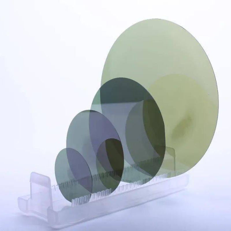
Chemical Mechanical Polishing (CMP) is a critical process in the semiconductor and microelectronics industry, where precision and smoothness are crucial for the manufacturing of advanced devices. As one of the industry leaders in CMP technology, {company name} has been revolutionizing the way semiconductor materials are polished to achieve superior surface quality and consistency.{Company name} is a globally recognized leader in CMP technology, with a strong focus on research and development to push the boundaries of innovation in semiconductor manufacturing. With a commitment to providing cutting-edge solutions for their customers, {company name} has become synonymous with excellence in CMP technology.As semiconductor devices become increasingly complex and advanced, the demand for higher precision and surface quality has never been greater. To meet these evolving needs, {company name} has continuously invested in advancing their CMP technology to deliver state-of-the-art solutions that enable their customers to achieve the highest levels of performance and reliability in their semiconductor devices.One of {company name}'s flagship products is their advanced CMP polishing pads, which are engineered to deliver exceptional planarity and uniformity, as well as reduced defectivity and improved yield. These polishing pads are designed to provide the highest level of performance, reliability, and cost-effectiveness, making them the preferred choice for leading semiconductor manufacturers around the world.In addition to their cutting-edge polishing pads, {company name} also offers a comprehensive range of CMP slurries, which are specially formulated to provide the optimal combination of selectivity, removal rate, and defectivity control. With their unparalleled expertise in material science and surface chemistry, {company name} is able to tailor their CMP slurries to meet the specific requirements of each customer, ensuring the highest level of performance and reliability in their semiconductor manufacturing processes.To complement their industry-leading products, {company name} also offers a range of CMP consumables, including conditioning disks, cleaning brushes, and carrier rings, which are essential for maintaining the performance and longevity of CMP equipment. These consumables are designed to deliver the highest levels of consistency and reliability, helping to maximize the efficiency and productivity of semiconductor manufacturing operations.One of the key differentiators of {company name} is their commitment to providing comprehensive technical support and customer service. Their team of highly skilled engineers and technicians work closely with customers to optimize their CMP processes, troubleshoot any issues, and ensure the highest level of performance and reliability in their semiconductor manufacturing operations. This dedication to customer satisfaction has earned {company name} a reputation as a trusted partner in the semiconductor industry.Looking ahead, {company name} is committed to continuing their tradition of innovation and excellence in CMP technology. With a strong focus on research and development, they are constantly pushing the boundaries of what is possible in semiconductor manufacturing, developing cutting-edge solutions that enable their customers to stay ahead of the curve in an ever-evolving industry.In conclusion, {company name} is a global leader in CMP technology, providing a comprehensive range of cutting-edge products and solutions for the semiconductor and microelectronics industry. With a strong focus on innovation, quality, and customer satisfaction, {company name} is at the forefront of driving the next generation of semiconductor manufacturing processes.

Read More

A Guide to Understanding Silicon Wafer Thickness

By:Admin on 2024-12-09 03:20:44

Silicon Wafer Thickness is a critical factor in the production of semiconductors and electronic devices. The thickness of the silicon wafer determines the performance and reliability of the final product. As technology advances, the demand for thinner silicon wafers has increased, driving the need for advanced manufacturing processes and quality control. One company at the forefront of this industry is {Company Name}.{Company Name} is a leading manufacturer of silicon wafers, specializing in ultra-thin wafer technology. Their state-of-the-art manufacturing facilities and cutting-edge research and development capabilities have positioned them as a key player in the semiconductor industry. With a focus on innovation and quality, {Company Name} has consistently delivered high-performance silicon wafers to their customers around the world.The thickness of silicon wafers is a critical parameter that directly impacts their electrical and mechanical properties. Thinner wafers offer advantages such as improved performance, reduced power consumption, and enhanced thermal management. However, manufacturing ultra-thin wafers presents its own set of challenges, including handling and processing issues. {Company Name} has overcome these challenges with their expertise and advanced manufacturing processes, allowing them to produce silicon wafers with thicknesses that were once thought to be impossible.In a recent breakthrough, {Company Name} announced the successful development of silicon wafers with an unprecedented thickness of less than 50 micrometers. This achievement positions {Company Name} as a leader in ultra-thin wafer technology and opens up new possibilities for the semiconductor industry. These ultra-thin wafers will enable the production of next-generation electronic devices with enhanced performance and efficiency.The development of ultra-thin silicon wafers is a game-changer for the semiconductor industry. It not only improves the performance of electronic devices but also reduces their environmental impact. Thinner wafers require less material, leading to reduced waste and lower manufacturing costs. This aligns with {Company Name}'s commitment to sustainability and corporate responsibility, making them a preferred partner for environmentally conscious customers.{Company Name} has invested heavily in research and development to push the boundaries of silicon wafer technology. Their team of experts continuously explores new materials, processes, and applications to stay at the forefront of the industry. By collaborating with leading semiconductor manufacturers, {Company Name} has gained valuable insights into the evolving needs of the market and has tailored their product offerings to meet these demands.As the demand for thinner silicon wafers continues to grow, {Company Name} is well-positioned to capitalize on this trend. Their proven track record in delivering high-quality, ultra-thin wafers, combined with their unwavering commitment to innovation, sets them apart in the competitive semiconductor market. With an eye on the future, {Company Name} is poised to drive the next wave of technological advancements through their pioneering work in silicon wafer thickness.In conclusion, the development of ultra-thin silicon wafers by {Company Name} marks a significant milestone in the semiconductor industry. Their relentless pursuit of innovation and excellence has propelled them to the forefront of ultra-thin wafer technology, setting new standards for performance and quality. As the demand for thinner wafers continues to rise, {Company Name} remains a trusted partner for semiconductor manufacturers looking to stay ahead of the curve. With their cutting-edge technology and commitment to sustainability, {Company Name} is shaping the future of electronic devices through their breakthroughs in silicon wafer thickness.

Read More