High-quality optical lenses for various applications

By:Admin on 2025-11-03 02:50:40

The global market for optical lenses is rapidly expanding, leading to technological advancements and innovative products by key industry players. One such company that has been at the forefront of this technological revolution is {}.{} is a leading manufacturer of optical lenses, specializing in the production of high-quality glass lenses for various applications. With a strong focus on research and development, the company has consistently introduced cutting-edge products that have set new benchmarks in the industry.The latest offering from {} is its range of Glass Optical Lenses, which have been designed to meet the growing demand for precision optics in a wide range of industries. These lenses are manufactured using state-of-the-art technology and advanced production processes, ensuring exceptional optical performance and durability.One of the key features of {}’s Glass Optical Lenses is their high light transmission, which is crucial for achieving superior image quality in applications such as microscopy, medical imaging, and industrial inspection. This is made possible by the use of premium quality glass materials that are carefully selected and processed to minimize light dispersion and maximize clarity.In addition to their optical performance, {}’s Glass Optical Lenses are also designed to be highly resistant to environmental factors such as temperature fluctuations and humidity. This makes them ideal for use in harsh operating conditions, where consistent optical performance is essential.The diverse range of Glass Optical Lenses offered by {} caters to the specific requirements of different industries, including but not limited to:- Microscopy: High-resolution lenses that enable detailed examination of microscopic specimens.- Medical Imaging: Lenses designed to deliver precise and accurate imaging for diagnostic purposes.- Industrial Inspection: Lenses that provide clear and accurate visualization for quality control and inspection processes.The superior quality and performance of {}’s Glass Optical Lenses have made them the preferred choice for leading companies and research institutions across the globe. These lenses have been instrumental in driving advancements in various fields, including medical research, materials science, and electronics manufacturing.Speaking about the company’s latest innovation, the CEO of {} stated, “We are thrilled to introduce our range of Glass Optical Lenses, which represent the culmination of years of research and development efforts. These lenses embody our commitment to excellence and innovation, and we are confident that they will set new standards for optical performance in the industry.”As part of its commitment to customer satisfaction, {} offers customization options for its Glass Optical Lenses, allowing clients to tailor the lenses to their specific requirements. This customization capability, combined with the company’s extensive technical expertise, has made {} a trusted partner for companies seeking high-performance optical solutions.Looking ahead, {} remains focused on pushing the boundaries of optical technology and providing customers with cutting-edge solutions that enable them to achieve their goals. With its innovative products and customer-centric approach, {} is well-positioned to maintain its leadership in the global optical lenses market.

Read More

New 12inch Substrate BF33 Unveiled: What You Need to Know

By:Admin on 2025-10-30 02:11:40

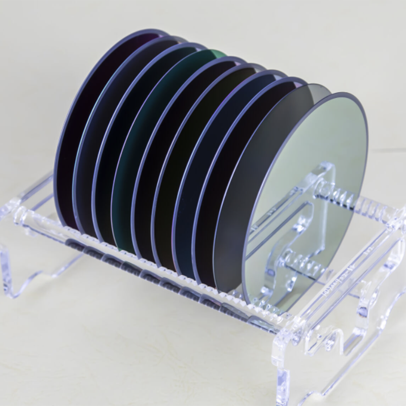
12inch BF33 Substrate: Revolutionizing Semiconductor ManufacturingIn today's fast-paced technological world, the demand for high-performance semiconductors is increasing exponentially. As the foundation of modern electronics, semiconductors play a crucial role in powering our smartphones, computers, and various other electronic devices. To meet this growing demand, semiconductor manufacturers are constantly striving to improve the performance and efficiency of their products. One company leading the charge in this endeavor is {}.{} is a leading manufacturer of advanced semiconductor materials and solutions. With a commitment to innovation and excellence, the company has been at the forefront of developing cutting-edge technologies that are revolutionizing the semiconductor industry. One of their most recent breakthroughs is the development of the 12inch BF33 substrate, a game-changing innovation that is set to redefine semiconductor manufacturing.The 12inch BF33 substrate is a revolutionary new material that offers unparalleled performance and efficiency for semiconductor manufacturing. With its high thermal conductivity and superior electrical properties, the BF33 substrate is capable of delivering significant improvements in device performance, power consumption, and overall reliability. This breakthrough technology is poised to address the growing demand for high-performance semiconductors in a wide range of applications, including 5G communications, artificial intelligence, and automotive electronics.The key advantage of the 12inch BF33 substrate lies in its ability to enhance the performance and efficiency of semiconductor devices. By enabling higher power densities and improved thermal management, the BF33 substrate allows for the development of highly efficient and reliable semiconductor products. This is particularly significant in the context of emerging technologies such as 5G, where the demand for high-speed, low-latency communication requires semiconductor devices to operate at unprecedented levels of performance.In addition to its superior performance characteristics, the 12inch BF33 substrate also offers cost-effective benefits for semiconductor manufacturers. The use of BF33 substrate can result in higher production yields and lower overall manufacturing costs, making it an attractive solution for companies looking to maximize their operational efficiency and profitability. Furthermore, the scalability of the BF33 substrate makes it suitable for a wide range of semiconductor applications, from power devices to radio frequency (RF) components.With the introduction of the 12inch BF33 substrate, {} is once again demonstrating its commitment to driving innovation and advancing the semiconductor industry. By leveraging their expertise in materials science and semiconductor manufacturing, the company is positioning itself as a leader in the development of advanced technologies that are shaping the future of electronics. As the demand for high-performance semiconductors continues to grow, the 12inch BF33 substrate is poised to play a vital role in meeting the evolving needs of the industry.In conclusion, the 12inch BF33 substrate represents a major milestone in the advancement of semiconductor manufacturing. With its unmatched performance, efficiency, and cost-effective benefits, this groundbreaking material is set to redefine the capabilities of semiconductor devices and drive the next wave of technological innovation. As {} continues to lead the way in developing cutting-edge semiconductor solutions, the 12inch BF33 substrate stands as a testament to the company's commitment to pushing the boundaries of what is possible in the world of electronics.

Read More

Dicing Process in Semiconductor Industry: Everything You Need to Know

By:Admin on 2025-10-27 02:51:58

Wafer Dicing, also known as die singulation, is a critical process in the semiconductor industry where a semiconductor wafer is diced into individual semiconductor chips. This process is essential for creating the microchips that are used in a wide range of electronic devices, including smartphones, computers, and other consumer electronics.{Company Name} is a leading provider of wafer dicing services, specializing in advanced wafer dicing solutions for the semiconductor industry. With state-of-the-art equipment and a team of highly skilled technicians, {Company Name} is dedicated to providing high-quality wafer dicing services to meet the growing demands of the semiconductor industry.The wafer dicing process involves cutting the semiconductor wafer into individual chips using a dicing saw. This process requires precision and accuracy to ensure that the individual chips are not damaged and can be used in electronic devices. {Company Name} has invested in cutting-edge dicing equipment and employs a team of experienced technicians to ensure that the dicing process is carried out with the highest level of precision and quality.In addition to wafer dicing services, {Company Name} also offers value-added services such as tape and reel packaging, laser marking, and visual inspection to provide comprehensive solutions for the semiconductor industry. These value-added services streamline the production process and ensure that the semiconductor chips are ready for use in electronic devices.{Company Name} prides itself on its commitment to quality and customer satisfaction. The company follows strict quality control procedures throughout the wafer dicing process to ensure that the semiconductor chips meet the highest industry standards. Additionally, {Company Name} works closely with its customers to understand their specific requirements and provide customized wafer dicing solutions to meet their unique needs.With the rapidly growing demand for semiconductor chips in electronic devices, {Company Name} has positioned itself as a reliable partner for semiconductor manufacturers seeking high-quality wafer dicing services. The company's dedication to innovation, quality, and customer satisfaction has earned it a reputation as a trusted provider of wafer dicing solutions in the semiconductor industry.As the semiconductor industry continues to evolve, {Company Name} remains at the forefront of technological advancements, constantly updating its equipment and processes to meet the changing demands of the industry. The company is committed to staying ahead of the curve and providing its customers with cutting-edge wafer dicing solutions to support their innovation in the semiconductor market.In conclusion, wafer dicing is a critical process in the semiconductor industry, and {Company Name} is dedicated to providing high-quality wafer dicing services to meet the growing demands of the industry. With its state-of-the-art equipment, skilled technicians, and commitment to quality, {Company Name} is well-positioned to be a leading provider of wafer dicing solutions for semiconductor manufacturers. The company's dedication to innovation and customer satisfaction sets it apart as a trusted partner in the semiconductor industry.

Read More