Sapphire Wafer for C-plane Axis: Recent Developments and Advancements

By:Admin on 2025-03-31 03:19:26

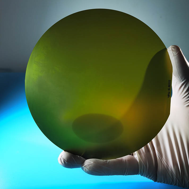
C-plane Axis Sapphire Wafer Leads the Industry in Sapphire Substrate TechnologySapphire is a highly versatile material that has become widely used in various industries, including semiconductor, aerospace, and defense. Its unique properties, such as high thermal conductivity, high strength, and optical transparency have made it an ideal material for applications that require high performance and reliability.A leading manufacturer in the sapphire substrate technology industry, C-plane Axis, has been at the forefront of developing high-quality sapphire wafers for a wide range of applications. Their innovative C-plane Axis sapphire wafer has set a new standard in the industry, offering unmatched performance and reliability.The company's C-plane Axis sapphire wafer is a result of years of research and development, and it represents a significant advancement in sapphire substrate technology. The wafer is produced using a proprietary process that ensures the highest level of quality and consistency. This process allows for precise control over the wafer's crystalline structure, which is essential for achieving superior mechanical and optical properties.One of the key features of the C-plane Axis sapphire wafer is its exceptional flatness and surface finish. This allows for better bonding and integration with other materials, making it an ideal choice for use in advanced semiconductor devices. The wafer also exhibits excellent optical clarity, making it suitable for applications in high-power LEDs, optical windows, and lenses.In addition to its superior physical properties, the C-plane Axis sapphire wafer also offers excellent thermal conductivity, which is critical for applications in high-power electronics and RF devices. The wafer's high thermal conductivity enables efficient heat dissipation, contributing to the overall performance and reliability of the devices in which it is used.Furthermore, the C-plane Axis sapphire wafer is available in a wide range of sizes and thicknesses, making it suitable for various manufacturing processes and applications. This flexibility allows for greater design freedom and customization, meeting the specific requirements of different industries and applications.Aside from its technical specifications, the C-plane Axis sapphire wafer is also produced with an environmentally friendly approach. The manufacturing process minimizes waste and energy consumption, aligning with the company's commitment to sustainability and responsible manufacturing practices.The C-plane Axis sapphire wafer has garnered international recognition and has been adopted by leading companies in the semiconductor, aerospace, and defense industries. Its superior performance and reliability have made it the preferred choice for demanding applications that require the highest level of quality and performance.C-plane Axis, the company behind the innovative sapphire wafer, is a global leader in sapphire substrate technology. With a strong focus on research and development, the company continues to push the boundaries of sapphire material science, driving innovation and excellence in the industry.Established in [year], C-plane Axis has built a solid reputation for delivering high-quality sapphire wafers that meet the stringent requirements of various industries. The company's state-of-the-art manufacturing facilities and advanced process technologies enable them to produce sapphire wafers with exceptional precision and performance.In addition to their cutting-edge products, C-plane Axis is committed to providing unparalleled customer support and technical expertise. Their team of highly skilled engineers and researchers work closely with customers to develop customized solutions that address their specific needs and requirements.As the demand for high-performance materials continues to grow, C-plane Axis remains dedicated to driving innovation and setting new standards in sapphire substrate technology. The company's C-plane Axis sapphire wafer stands as a testament to their commitment to excellence and their ability to deliver superior products that meet the evolving needs of the industry.In conclusion, the C-plane Axis sapphire wafer represents a significant advancement in sapphire substrate technology, offering unmatched performance and reliability for a wide range of applications. With its superior physical properties, environmentally friendly manufacturing process, and exceptional technical support, C-plane Axis continues to lead the industry in sapphire material science, driving innovation and excellence in the field.

Read More

Key Developments in the 300mm Semiconductor Industry: All You Need to Know

By:Admin on 2025-03-27 02:27:00

The semiconductor industry is constantly evolving, and advancements in technology continue to drive innovation. One such advancement comes in the form of 300mm semiconductor technology, which has the potential to revolutionize the way we think about microelectronics. This technology, developed by [Company], has the power to significantly increase the efficiency and performance of semiconductor devices, paving the way for new and improved electronic products.[Company] is a leading global technology company that is at the forefront of semiconductor innovation. With a strong focus on research and development, [Company] has been able to leverage its expertise to create cutting-edge 300mm semiconductor technology. This technology allows for the manufacturing of larger wafers, providing more space for the integration of complex circuits and components. As a result, semiconductor devices produced using 300mm technology are smaller, more powerful, and more energy-efficient than their predecessors.The benefits of 300mm semiconductor technology are far-reaching. For one, it enables the production of advanced microprocessors, memory chips, and other semiconductor devices that are vital components of electronic products such as smartphones, computers, and IoT devices. The larger wafers also lead to increased economies of scale, lowering the cost of production and making semiconductor devices more affordable for consumers.Furthermore, 300mm semiconductor technology facilitates the development of new and innovative electronic products that were previously not feasible. For instance, it opens up possibilities for the creation of more compact and high-performance medical devices, automotive electronics, and smart home appliances. These advancements have the potential to improve the quality of life for individuals and drive progress across various industries.In addition to its technological advancements, [Company] is committed to sustainability and environmental responsibility. The 300mm semiconductor technology aligns with these values by enabling more energy-efficient semiconductor devices. This, in turn, contributes to reducing energy consumption and lowering carbon emissions, making a positive impact on the environment.Furthermore, [Company] takes pride in its dedication to quality and reliability. The 300mm semiconductor technology undergoes rigorous testing and validation to ensure that the semiconductor devices produced are of the highest standard. This commitment to quality positions [Company] as a trusted partner for businesses seeking reliable semiconductor solutions.With the global demand for high-performance electronic products on the rise, the 300mm semiconductor technology developed by [Company] has the potential to disrupt the semiconductor industry. Its ability to drive innovation, improve efficiency, and reduce costs makes it a game-changer in the world of microelectronics.Industry experts have recognized the significance of 300mm semiconductor technology, with many touting it as the future of semiconductor manufacturing. As the industry continues to evolve, [Company] is well-positioned to lead the way in the development and commercialization of this revolutionary technology.In conclusion, the 300mm semiconductor technology developed by [Company] has the potential to transform the semiconductor industry and drive innovation across various electronic products. With its focus on research and development, commitment to sustainability, and dedication to quality, [Company] is poised to make a significant impact in the world of microelectronics. As the demand for high-performance electronic products continues to grow, the 300mm semiconductor technology stands ready to meet the needs of consumers and businesses alike.

Read More

High-Quality LiNbO3 Wafer Supplier for Advanced Electronics Applications

By:Admin on 2025-03-24 03:19:51

In the world of technology, the demand for high-performance and reliable materials is constantly growing. Because of this, the significance of cutting-edge materials such as LiNbO3 wafers has become more evident than ever before. LiNbO3 wafers are a crucial component in a wide range of electronic devices, including high-frequency oscillators, surface acoustic wave devices, and electro-optic devices. This versatile material has gained attention for its exceptional electrical, optical, and physical properties, making it an essential element in the development of advanced technological applications.One company that has been leading the way in the production and development of LiNbO3 wafers is {Company Introduction}. With their expertise in crystal growth and precision machining, they have been able to produce high-quality LiNbO3 wafers that meet the demanding requirements of the industry. From research institutions to commercial enterprises, {Company Introduction} has been providing tailored solutions to various technological advancements.The unique properties of LiNbO3 wafers make them ideal for a wide range of applications. As a piezoelectric material, LiNbO3 wafers can efficiently convert electrical signals into mechanical vibrations and vice versa, making them essential in the development of high-frequency oscillators and surface acoustic wave devices. Additionally, the electro-optic properties of LiNbO3 wafers allow for the modulation and manipulation of light, making them crucial in the development of optical devices such as modulators and switches.With a focus on quality and innovation, {Company Introduction} has positioned itself as a leading supplier of LiNbO3 wafers in the global market. Their commitment to research and development has led to the continuous improvement of their products, ensuring that they meet the evolving demands of the industry. By leveraging their expertise in crystal growth and precision machining, they have been able to produce LiNbO3 wafers with exceptional electrical, optical, and physical properties, making them a preferred choice for many technological applications.The growing demand for LiNbO3 wafers has presented {Company Introduction} with opportunities to expand their market reach and collaborate with various industries. Their dedication to customer satisfaction and technical support has earned them a solid reputation in the industry, allowing them to build strong partnerships with clients across different sectors. Whether it is for research and development or commercial production, {Company Introduction} has been able to offer tailored solutions to meet the specific requirements of their customers.As technology continues to advance, the role of LiNbO3 wafers in electronic devices and optical applications will become increasingly critical. {Company Introduction} is well-positioned to capitalize on this trend, with their focus on quality, innovation, and customer satisfaction. Their commitment to pushing the boundaries of crystal growth and precision machining has allowed them to stay at the forefront of the industry, providing high-performance LiNbO3 wafers that empower technological advancements across the globe.In conclusion, LiNbO3 wafers play a crucial role in the development of advanced electronic and optical devices, and {Company Introduction} has emerged as a key player in the production and supply of these essential materials. With their dedication to quality, innovation, and customer satisfaction, {Company Introduction} has positioned itself as a trusted partner for businesses and research institutions seeking high-performance LiNbO3 wafers. As the demand for advanced materials continues to grow, {Company Introduction} remains committed to pushing the boundaries of crystal growth and precision machining, ensuring that they continue to meet the evolving needs of the industry.

Read More