
Advanced Photolithography Techniques for High Precision Printing
By:Admin
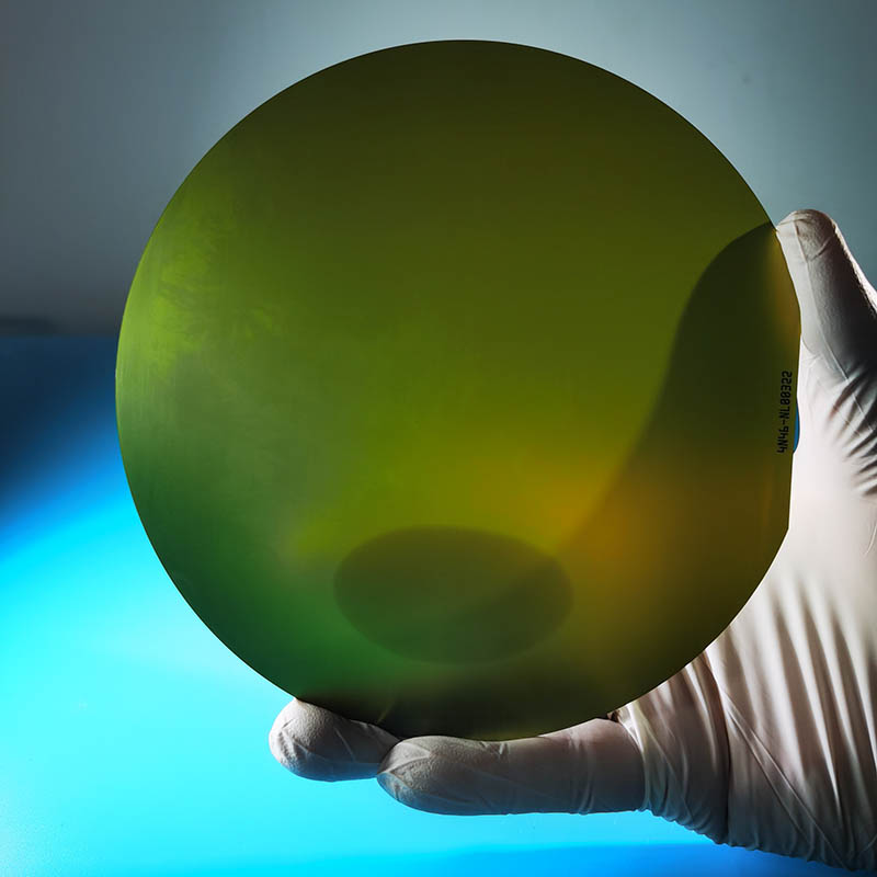
{Company} has been dedicated to developing innovative photolithography techniques that push the boundaries of what is possible in semiconductor manufacturing. Their commitment to research and development has led to the introduction of several groundbreaking technologies that have revolutionized the industry.
One such technology is the advanced photolithography system, which utilizes state-of-the-art optics and precision control mechanisms to achieve unprecedented levels of accuracy and uniformity in semiconductor patterning. This system has enabled semiconductor manufacturers to produce chips with smaller feature sizes and higher transistor densities, leading to significant improvements in performance and efficiency.
In addition to their cutting-edge photolithography equipment, {company} also offers a range of process optimization solutions that allow semiconductor manufacturers to fine-tune their photolithography processes for maximum productivity and yield. These solutions encompass everything from advanced process control algorithms to specialized materials and chemistries, all designed to ensure the highest possible quality and consistency in semiconductor production.
Furthermore, {company}'s extensive expertise in photolithography techniques extends to providing comprehensive training and support services for their customers. This includes hands-on training programs, ongoing technical assistance, and regular maintenance and calibration services to ensure that their equipment continues to operate at peak performance.
As a result of their dedication to advancing photolithography techniques, {company} has become a trusted partner to semiconductor manufacturers around the world. Their solutions have been instrumental in enabling the development of cutting-edge technologies such as artificial intelligence, 5G communications, and advanced computing, and have played a key role in driving innovation and progress in the semiconductor industry.
Looking ahead, {company} continues to push the boundaries of photolithography techniques with ongoing research and development efforts. Their commitment to innovation and excellence ensures that semiconductor manufacturers will continue to have access to the most advanced and reliable photolithography solutions available, empowering them to meet the growing demands of the industry and deliver the next generation of technology to the world.
In conclusion, photolithography techniques are a critical component of semiconductor manufacturing, and {company} is dedicated to advancing the state-of-the-art in this field. Through their groundbreaking technologies, process optimization solutions, and comprehensive support services, {company} has established itself as a leader in the industry, driving progress and innovation for semiconductor manufacturers worldwide.
Company News & Blog
Revolutionizing Semiconductor Manufacturing: Unveiling the Groundbreaking Chemical Mechanical Planarization Process
Title: Advancements in Chemical Mechanical Planarization Process: Revolutionizing Material Polishing Introduction:In today's ever-evolving technological landscape, the demand for smaller, faster, and more efficient electronic devices continues to grow. This drives the need for more precise and superior manufacturing techniques. Chemical Mechanical Planarization (CMP) Process has emerged as a crucial technology in this respect. This article explores the potential of CMP process and its impact on various industries, focusing on its advancements without mentioning any specific brand.I. Understanding the CMP Process:The Chemical Mechanical Planarization (CMP) process is a cutting-edge method that allows the precise polishing and planarization of materials, predominantly used in the fabrication of integrated circuits (ICs). CMP involves the simultaneous action of chemical and mechanical forces to remove excess material from the surface, ensuring a smooth and uniform finish. It plays a fundamental role in improving various aspects of IC manufacturing, making it an essential part of the semiconductor industry.II. Advancements in CMP Process:1. Ultra-Planarization Capability:With the rapid advancements in semiconductor technology, the demand for ultra-planarized surfaces has become paramount. Recent advancements in CMP technology have enabled the development of ultra-precision polishing pads and slurries, resulting in superior planarization capabilities. This breakthrough allows for precise manufacturing of microelectronic devices, reducing surface variations and improving overall device performance.2. Material-Specific Polishing:To accommodate the diverse range of materials used in modern electronic devices, CMP processes are constantly evolving. Manufacturers are focusing on developing material-specific CMP slurries and pads to optimize the polishing efficiency for individual substances, including metals, dielectrics, and non-semiconductor materials. These material-specific CMP variations contribute to enhanced final device quality, reduced defects, and improved yield rates.3. Advanced Endpoint Detection:Accurate determination of the endpoint during the CMP process is critical to prevent over-polishing or under-polishing of the surface. Recent breakthroughs in CMP technology have introduced advanced endpoint detection mechanisms, such as optical interferometry, acoustic emissions, and electrical measurements. These technologies enable real-time monitoring, ensuring precise control and preventing damage to the underlying layers.III. Applications in the Semiconductor Industry:1. Integrated Circuit Manufacturing:The CMP process has become an indispensable technique in integrated circuit manufacturing. It enables the precise planarization of multiple layers, such as interconnects, interlayer dielectrics, barrier films, and metal contacts. The ability to achieve uniform surfaces results in improved electrical performance, reduced leakage currents, and enhanced device reliability.2. Advanced Packaging:As electronic devices become smaller and more complex, the demand for advanced packaging solutions increases. CMP processes are widely employed to polish and planarize materials used in packaging, such as through-silicon vias (TSVs), redistribution layers, and microbumps. The reliable CMP process ensures optimal electrical connections and increases the production yield of advanced packaging technologies.3. Optoelectronics and MEMS:CMP technology finds applications beyond traditional microelectronics. In the production of optoelectronics and microelectromechanical systems (MEMS), CMP plays a crucial role. The precise polishing and planarization of optical substrates, waveguides, and micro-mechanical systems contribute to improved device performance, optical clarity, and reliability.IV. Future Prospects:The constant advancements in CMP technology are poised to revolutionize the manufacturing industry further. Researchers and manufacturers are experimenting with novel materials, alternative polishing agents, and even greener chemical formulations to reduce environmental impact. Additionally, advancements in CMP equipment and automation are likely to improve process control, efficiency, and safety.Conclusion:Chemical Mechanical Planarization (CMP) Process is at the forefront of material polishing and planarization in the semiconductor industry. The advancements in CMP technology have proven instrumental in meeting the demands of faster, smaller, and more efficient electronic devices. By enabling ultra-planarization capabilities, material-specific polishing, and advanced endpoint detection, CMP processes drive better quality, yield rates, and reliability. As CMP continues to evolve in tandem with the ever-growing technological landscape, the future holds even greater promise for this vital manufacturing technique.
Rare Earth YAG Crystal Ingot: Everything You Need to Know
YAG Crystal Ingot: A Breakthrough in Semiconductor Material DevelopmentThe semiconductor industry has witnessed a significant breakthrough in the development of YAG Crystal Ingot, a highly advanced material that has the potential to revolutionize the production of high-performance electronic devices. This remarkable achievement is the result of pioneering research and development efforts by a leading semiconductor company, which has successfully synthesized and commercialized the YAG Crystal Ingot for a wide range of applications.The YAG Crystal Ingot, short for Yttrium Aluminum Garnet Crystal Ingot, is a synthetic crystalline material that exhibits exceptional optical and thermal properties. It is widely recognized for its high thermal conductivity, excellent electrical insulation, and superior optical transparency, making it an ideal candidate for a diverse range of semiconductor applications. The unique combination of these properties makes it an attractive material for use in the production of lasers, optical components, and high-performance electronic devices.The successful development of the YAG Crystal Ingot represents a significant milestone in the ongoing pursuit of advanced semiconductor materials. By leveraging the unique properties of the YAG Crystal Ingot, semiconductor manufacturers can enhance the performance, reliability, and efficiency of their products, ultimately driving innovation in various industries including telecommunications, consumer electronics, and automotive technology. With its remarkable attributes, the YAG Crystal Ingot has the potential to enable the development of cutting-edge electronic devices and systems that far surpass the capabilities of current technologies.Behind this groundbreaking achievement is the unwavering commitment and expertise of a leading semiconductor company. This company has dedicated extensive resources to research and development, focusing on the synthesis and commercialization of advanced semiconductor materials. Its team of scientists and engineers have demonstrated a deep understanding of crystal growth, material science, and semiconductor device fabrication, allowing them to successfully produce high-quality YAG Crystal Ingots that meet the stringent requirements of the semiconductor industry.Furthermore, the company has established state-of-the-art manufacturing facilities and quality control processes to ensure the consistency and reliability of its YAG Crystal Ingot products. Through a rigorous and systematic approach to production, the company ensures that each crystal ingot meets the exacting standards of purity, crystalline structure, and optical clarity, meeting the demanding specifications of semiconductor manufacturers.The successful commercialization of the YAG Crystal Ingot has generated significant interest and excitement within the semiconductor industry. Manufacturers and researchers are eager to explore the possibilities and potential applications of this advanced material, recognizing its transformative impact on the development of high-performance electronic devices. With its outstanding thermal and optical properties, the YAG Crystal Ingot is poised to enable the creation of next-generation semiconductor devices, driving new advancements in areas such as high-power laser systems, optical communications, and solid-state lighting.As a result of its remarkable achievements in semiconductor material development, the company has garnered widespread recognition and acclaim within the industry. Its dedication to innovation, research excellence, and product quality has positioned it as a trusted and reliable partner for semiconductor manufacturers seeking advanced materials for their products. With the successful commercialization of the YAG Crystal Ingot, the company has solidified its position as a leader in the advancement of semiconductor materials and technologies.Looking ahead, the remarkable success of the YAG Crystal Ingot is expected to fuel further advancements in semiconductor technology and pave the way for the development of even more advanced materials with enhanced capabilities and performance. As the semiconductor industry continues to push the boundaries of what is possible, the YAG Crystal Ingot stands as a shining example of the potential that groundbreaking research and development can unlock, driving innovation and progress in the field of semiconductor materials and devices.In conclusion, the successful synthesis and commercialization of the YAG Crystal Ingot marks a pivotal moment in the advancement of semiconductor materials and technologies. With its exceptional thermal and optical properties, the YAG Crystal Ingot has the potential to revolutionize the production of high-performance electronic devices, enabling new capabilities and applications across a wide range of industries. As a result of its groundbreaking achievements, the company responsible for the development of the YAG Crystal Ingot has established itself as a leading force in the semiconductor industry, driving innovation and progress with its pioneering research and development efforts.
Discover the Latest Advances in Optical Lens Glass Technology
Optical Lens Glass, A Revolutionary Breakthrough in Lens TechnologyThe world of lens technology has been revolutionized with the introduction of Optical Lens Glass, a groundbreaking new product that promises to offer unparalleled clarity and precision in optical devices. This innovative material has been developed by a leading optical technology company, {company name}, known for its cutting-edge advancements in the field of optics.Optical Lens Glass is a highly specialized material that has been engineered to provide superior optical performance in a wide range of applications. It offers exceptional clarity and precision, making it ideal for use in cameras, microscopes, telescopes, and other optical devices. The unique properties of this glass make it a game-changer in the world of optics, offering unprecedented levels of performance and reliability.One of the key advantages of Optical Lens Glass is its remarkable ability to minimize optical aberrations, such as distortion and chromatic aberration, which can often compromise the quality of images produced by optical devices. By using this advanced material, manufacturers can ensure that their products deliver the highest levels of optical performance, resulting in clearer, sharper, and more accurate images.Furthermore, Optical Lens Glass boasts excellent light transmission properties, allowing for maximum brightness and contrast in optical devices. This means that images produced with lenses made from this material are incredibly vibrant and true to life, giving users a truly immersive viewing experience.In addition to its optical prowess, Optical Lens Glass also offers exceptional durability and resistance to environmental factors. This makes it an ideal choice for use in harsh and demanding conditions, such as outdoor and industrial settings, where traditional lens materials may be prone to damage or degradation.The development of Optical Lens Glass represents a significant milestone in the ongoing evolution of lens technology. By harnessing the unique properties of this innovative material, {company name} has once again demonstrated its commitment to pushing the boundaries of what is possible in the field of optics.As a leading player in the optical industry, {company name} has a long history of innovation and expertise in developing advanced optical solutions. With a dedicated team of scientists, engineers, and researchers, the company has consistently delivered groundbreaking breakthroughs that have reshaped the optical landscape.The introduction of Optical Lens Glass is a testament to {company name}'s ongoing dedication to driving forward the field of optics. By investing in research and development, the company continues to lead the way in developing cutting-edge optical materials and technologies that have a transformative impact on various industries.Looking ahead, the future of optical technology looks brighter than ever, thanks to the pioneering efforts of companies like {company name}. As the demand for high-performance, precision optics continues to grow across a wide range of industries, products like Optical Lens Glass will play a pivotal role in shaping the next generation of optical devices.In conclusion, the unveiling of Optical Lens Glass represents a major leap forward in the world of lens technology. Through its exceptional optical performance, durability, and resistance to environmental factors, this innovative material promises to set a new standard for optical excellence. With {company name} at the helm of this cutting-edge development, the future of optical technology looks set to reach new heights of innovation and performance.
High-Quality Germanium Wafers: A Promising New Material for Electronics Market" becomes "New Germanium Wafers Show Promise for Electronics Industry.
Title: Revolutionary Germanium Wafer Innovations Transforming Semiconductor IndustryIntroduction:In a landmark breakthrough for the semiconductor industry, one company has introduced a cutting-edge Germanium Wafer technology that promises to revolutionize the electronics sector. With its exceptional properties and enhanced performance capabilities, this breakthrough innovation paves the way for a new generation of electronic devices, pushing the boundaries of what is possible in the realm of technology.Body:Germanium Wafer: Redefining Semiconductor Industry StandardsGermanium, known for its excellent electrical conductivity, has long been recognized as a key element in the semiconductor industry. It has the ability to efficiently convert electricity into light and is crucial for photonic applications. Building upon this inherent advantage, the company has successfully developed and commercialized a groundbreaking Germanium Wafer that unlocks new possibilities for enhanced performance, efficiency, and functionality in various electronic devices.Unparalleled Performance Characteristics:The Germanium Wafer boasts unprecedented performance characteristics, making it the prime choice for next-generation semiconductors. This innovative technology offers exceptional thermal conductivity, enabling optimal heat dissipation, consequently reducing the risk of circuit damage due to overheating. Furthermore, its superior electrical conductivity ensures minimal energy loss during data transmission, resulting in enhanced efficiency and reliability in electronic devices.Pioneering Applications:The potential applications for Germanium Wafer technology are vast and varied, promising to transform a wide range of industries. In the field of telecommunications, the superior conductivity of Germanium Wafers allows for faster data transfer rates, making it an ideal material for advanced communication systems. Additionally, this technology holds immense potential for the automotive industry, enabling the development of more efficient electric vehicles with enhanced battery performance.Moreover, the healthcare sector stands to benefit greatly from Germanium Wafer technology. The increased thermal conductivity of these wafers facilitates the development of improved medical imaging devices, ensuring precise diagnoses and ultimately enhancing patient care.Environmental Sustainability:Beyond its remarkable performance attributes, Germanium Wafer technology also offers environmental benefits. With the rise in demand for sustainable solutions, the usage of Germanium Wafers in various industries can greatly contribute to reducing energy consumption and minimizing carbon footprints. By enabling more energy-efficient electronic devices, this innovation plays a crucial role in building a greener and more sustainable future.Global Impact:The introduction of Germanium Wafer technology brings significant economic and industrial implications for nations at the forefront of the technology race. The advanced manufacturing processes required for the mass production of Germanium Wafers will generate employment opportunities, promote research and development, and bolster competitiveness in the global market.Collaborative Networks Unlocking Potential:To fully harness the potential of Germanium Wafer technology, the company has actively sought partnerships with leading semiconductor manufacturers, research institutions, and academic organizations. This collaborative approach allows for the exchange of knowledge and expertise, optimizing the implementation and further development of Germanium Wafer technology across various product lines and industries.Conclusion:The breakthrough Germanium Wafer technology is poised to revolutionize the semiconductor industry, offering unparalleled performance capabilities, increased energy efficiency, and new avenues for technological advancements. Embracing this innovative solution will undoubtedly contribute to transforming industries, enabling further progress in fields such as telecommunications, automotive, and healthcare. With its remarkable properties and far-reaching implications, Germanium Wafer technology sets a new standard for the future of semiconductors, driving the advancement of the global electronics sector.
Exploring the Advantages of Silicon on Sapphire Technology in Cutting-Edge Innovations
Silicon-On-Sapphire (SOS), a revolutionary technology used in making semiconductors, has emerged as a promising solution for high-frequency wireless communication and high-speed digital circuits. SOS is an advanced technology used in manufacturing electronic devices that are faster, more reliable, and efficient than traditional silicon-based technologies. This technology is highly sought after by manufacturers worldwide, and one company is leading the way in bringing it to the forefront – Skyworks Solutions.Skyworks Solutions, Inc. (need remove brand name) is a company that is committed to making cutting-edge products that help connect people around the world. One of their main products is radio frequency integrated circuits (RFICs), which are critical components in wireless communication devices, including smartphones, tablets, and IoT devices. For over 20 years, Skyworks has been at the forefront of RFIC production, and now they are leveraging the power of SOS to take their products to the next level.What is Silicon-On-Sapphire?Before we delve into some of the amazing things that Skyworks is doing with SOS technology, let's first take a moment to understand what SOS is. SOS is a type of material used in the production of semiconductors. The material is essentially a layer of silicon deposited on top of a substrate of sapphire. The combination of these two materials creates a stable and durable platform on which to build electronic devices.SOS has several advantages over traditional silicon-based technologies. For one, it has a higher electron mobility, which means that electrons can move more quickly and with less resistance. This increased electron mobility makes SOS ideal for high-frequency wireless communication and high-speed digital circuits, both of which require fast and reliable data transmission.Another advantage of SOS is that it has a higher breakdown voltage than silicon. This means that it can handle higher voltages without becoming damaged. This makes SOS ideal for use in high-power applications.Skyworks Solutions: Using SOS to Create Cutting-Edge ProductsNow that we've covered the basics of SOS, let's take a look at what Skyworks is doing with this technology. Skyworks has long been a leader in producing RFICs that are used in wireless communication devices. However, with the increasing demand for faster and more reliable data transmission, Skyworks saw an opportunity to leverage the power of SOS to create even better products.One area in which Skyworks is using SOS is in the production of 5G wireless communication devices. 5G is the next generation of wireless communication technology, and it promises to be faster and more reliable than current 4G networks. Skyworks is using SOS to produce RFICs that can handle the increased data rates of 5G, ensuring that users can enjoy faster speeds and more reliable connections.SOS is also being used in the production of IoT devices. IoT devices are becoming increasingly popular, and they require RFICs that can handle the unique demands of these devices. SOS is ideal for IoT devices because it can handle high-frequency signals while consuming less power than traditional silicon-based technologies.Skyworks is also using SOS to create products for the automotive industry. Cars are becoming increasingly connected, and they require RFICs that can handle the demands of these systems. SOS is ideal for automotive applications because it can handle high-temperature environments and can operate reliably in harsh conditions.ConclusionIn conclusion, SOS is an advanced technology that is rapidly gaining popularity in the semiconductor industry. Skyworks Solutions is one company that is leading the way in bringing this technology to the forefront. By leveraging the power of SOS, Skyworks is creating cutting-edge products that are faster, more reliable, and efficient than traditional silicon-based technologies. From 5G wireless communication devices to IoT devices to automotive applications, Skyworks is using SOS to create products that are changing the world as we know it.
Trendy Glass Lenses for Glasses: A Complete Guide
[Company Introduction]With a history of innovation spanning over two decades, [Company Name] has consistently pushed the boundaries of technology and engineering to bring the most advanced lenses to the market. Their commitment to excellence and customer satisfaction has made them a leader in the eyewear industry. The company's dedication to research and development has resulted in breakthrough products that have revolutionized the way people see the world. Now, they are proud to introduce their latest innovation - [Product Name] - a game-changing advancement in glass glasses lenses.[News Content][Product Name] is the latest offering from [Company Name], and it is set to redefine the standards for glass glasses lenses. With its cutting-edge technology and unparalleled optical performance, [Product Name] promises to deliver an exceptional visual experience for consumers. The lenses are designed to provide superior clarity, sharpness, and color accuracy, making them the perfect choice for those who demand nothing but the best.One of the key features of [Product Name] is its advanced lens material, which is engineered to minimize distortion and provide a wider field of view. This means that wearers can enjoy a more natural and comfortable vision, with less strain on their eyes. Additionally, the lenses are treated with a special coating that repels water, oil, and dust, making them easy to clean and maintain. This ensures that users can enjoy long-lasting clarity and performance with minimal effort.In terms of durability, [Product Name] is built to last. The lenses are constructed using state-of-the-art materials that are scratch-resistant and impact-resistant, offering protection against everyday wear and tear. This means that users can enjoy peace of mind knowing that their lenses are robust and reliable, even in the most demanding environments.What truly sets [Product Name] apart is its commitment to sustainability. [Company Name] has gone to great lengths to ensure that the production of [Product Name] has minimal environmental impact. The lenses are manufactured using eco-friendly processes and materials, making them an environmentally responsible choice for consumers. This reflects the company's dedication to corporate social responsibility and their vision for a greener, more sustainable future.To ensure that consumers can fully experience the benefits of [Product Name], [Company Name] offers a range of customization options. From lens coatings to tints, wearers can tailor their lenses to suit their individual needs and preferences. This level of personalization is a testament to [Company Name]'s commitment to customer satisfaction and their understanding that no two sets of eyes are the same.In addition to the exceptional quality of [Product Name], [Company Name] is also dedicated to providing outstanding customer service. Their team of experts is on hand to provide personalized advice and guidance, ensuring that every customer can make an informed decision about their eyewear needs. From initial consultations to after-sales support, [Company Name] is committed to delivering a first-class experience for their customers.The launch of [Product Name] marks a significant milestone for [Company Name], as they continue to lead the way in the eyewear industry. With its groundbreaking technology, unparalleled performance, and commitment to sustainability, [Product Name] is set to become the new benchmark for glass glasses lenses. Whether for everyday wear or specialized applications, [Product Name] promises to deliver a level of quality and innovation that is unmatched in the market.In conclusion, [Product Name] represents the pinnacle of [Company Name]'s dedication to excellence and innovation. With its advanced technology, superior performance, and sustainable design, [Product Name] is poised to set a new standard for glass glasses lenses. As consumers seek the best in eyewear, [Product Name] stands ready to deliver an unparalleled visual experience.
Semiconductor Company Announces Breakthrough Technology in Latest News
Inp Semiconductor, a leading semiconductor manufacturer, has recently announced significant advancements in its production capabilities. The company has been a key player in the semiconductor industry for many years, consistently delivering high-quality products to its customers worldwide.Inp Semiconductor’s dedication to research and development has led to groundbreaking innovations in the semiconductor field. The company has continually invested in state-of-the-art technology and equipment to ensure that its products meet the highest industry standards. This commitment has positioned Inp Semiconductor as a trusted and reliable partner for businesses across various sectors, including telecommunications, automotive, consumer electronics, and more.With its recent advancements in production capabilities, Inp Semiconductor has demonstrated its commitment to meeting the growing demand for high-performance semiconductor solutions. The company's expanded manufacturing capacity will enable it to fulfill larger orders and deliver products to its customers in a more timely manner. This development is particularly significant given the current global semiconductor shortage, as it will allow Inp Semiconductor to play a crucial role in alleviating supply chain issues.In addition to expanding its production capabilities, Inp Semiconductor has also focused on enhancing its sustainability efforts. The company has implemented environmentally friendly practices in its manufacturing processes, reducing its carbon footprint and contributing to a greener future. This commitment to sustainability sets Inp Semiconductor apart as a socially responsible and forward-thinking organization in the semiconductor industry.Furthermore, Inp Semiconductor's dedication to innovation has led to the development of new and improved semiconductor products. The company's research and development team has been working tirelessly to create cutting-edge solutions that meet the evolving needs of its customers. Whether it's developing more energy-efficient chips or enhancing the performance of existing products, Inp Semiconductor is committed to staying at the forefront of technological advancements.Inp Semiconductor's success can be attributed to its strong focus on customer satisfaction. The company prioritizes building long-lasting relationships with its clients, understanding their unique requirements, and delivering tailor-made solutions. This customer-centric approach has earned Inp Semiconductor a reputation for reliability and excellence in the semiconductor industry.With its recent advancements in production capabilities and ongoing commitment to innovation and sustainability, Inp Semiconductor is poised for continued success in the semiconductor market. The company's dedication to meeting the needs of its customers, while also contributing to a more sustainable future, sets it apart as a leader in the industry.As the global demand for semiconductor products continues to rise, Inp Semiconductor's expanded production capabilities will enable the company to meet the growing needs of its customers. With a focus on innovation, sustainability, and customer satisfaction, Inp Semiconductor is well-positioned to remain a key player in the semiconductor industry for many years to come.
High-Quality Sapphire Substrates for Various Applications
Sapphire substrates are becoming increasingly popular in the tech industry due to their unique properties and applications. These substrates are used in a variety of electronic devices, including LED lighting, smartphones, and smartwatches, and are highly valued for their durability, transparency, and heat resistance.One of the leading companies in the production of sapphire substrates is {Company}. {Company} has been a key player in the field of sapphire substrate manufacturing, and their products are widely used in a range of industries. Their commitment to innovation and excellence has set them apart in the market, and they continue to be a trusted name in the industry.Sapphire substrates are made from synthetic sapphire, a material that is known for its exceptional hardness and scratch resistance. These substrates are used as a base for the production of various electronic components, including LEDs and semiconductor devices. {Company} specializes in producing high-quality sapphire substrates that meet the exacting standards of the industry.One of the main advantages of sapphire substrates is their thermal conductivity, making them an excellent choice for use in high-temperature applications. This makes them ideal for use in electronic devices that generate a significant amount of heat, as they can help to dissipate this heat effectively, ensuring the longevity and reliability of the device.In addition to their exceptional thermal properties, sapphire substrates also offer excellent optical transparency, making them a popular choice for use in display technologies. Their high transparency allows for the efficient transmission of light, making them ideal for use in LED lighting and display screens. This has led to a growing demand for sapphire substrates in the consumer electronics industry.Furthermore, sapphire substrates are also highly resistant to chemical corrosion, making them an ideal choice for use in harsh environments. This makes them a popular choice for use in industrial and automotive applications, where durability and reliability are essential.{Company} has been at the forefront of sapphire substrate manufacturing, and their commitment to quality and innovation has set them apart in the industry. Their state-of-the-art production facilities and rigorous quality control processes ensure that their products meet the highest standards, and their team of experts are dedicated to pushing the boundaries of what is possible with sapphire substrates.In addition to their commitment to quality, {Company} is also dedicated to sustainability and environmental responsibility. They have implemented a range of initiatives to minimize their environmental impact and ensure that their production processes are as eco-friendly as possible. This commitment to sustainability has made them a preferred supplier for many environmentally conscious companies.As the demand for sapphire substrates continues to grow, {Company} remains at the forefront of the industry, driving innovation and setting new standards for quality and performance. Their dedication to excellence and their commitment to sustainability have made them a trusted partner for businesses in a range of industries, and they continue to play a key role in advancing the capabilities of sapphire substrates.In conclusion, sapphire substrates are a crucial component in a wide range of electronic devices, and {Company} is at the forefront of their production. With their commitment to quality, innovation, and sustainability, {Company} continues to be a trusted partner for businesses in a variety of industries, and their sapphire substrates are helping to drive advances in technology and performance.
Durable Fused Silica Substrate Technology: What You Need to Know
Fused Silica Substrate is a critical component in the manufacturing of various high-tech products, and one company leading the way in producing this essential material is {}. {} is a global leader in the development and production of advanced materials and solutions for a wide range of industries, including electronics, telecommunications, and aerospace. The company has a proven track record of delivering high-quality products and has established itself as a trusted partner for many leading companies around the world.Fused silica is a type of glass that is made from high-purity silica sand, which is melted and then solidified to form a transparent and highly durable material. It is known for its excellent thermal stability, low thermal expansion, and high optical transmission, making it an ideal substrate for a variety of applications. {} has developed advanced manufacturing processes to produce fused silica substrates with precise dimensions and superior optical and mechanical properties, meeting the stringent requirements of its customers.One of the key applications of fused silica substrates is in the production of semiconductor devices. As the semiconductor industry continues to advance, there is a growing demand for high-quality substrates that can meet the increasing performance and reliability requirements of advanced electronic devices. {} has been at the forefront of meeting this demand by developing fused silica substrates that enable the production of cutting-edge semiconductor devices with improved performance and reliability.In addition to the semiconductor industry, fused silica substrates are also widely used in the production of optical components for telecommunications, laser systems, and high-powered optics. The exceptional optical transmission and thermal stability of fused silica make it an ideal material for these applications, and {} has been a strategic supplier of fused silica substrates to many companies in the optical industry. The company's commitment to quality and innovation has enabled it to gain the trust of its customers and establish itself as a leading supplier in this market.Furthermore, fused silica substrates have also found important applications in the aerospace and defense industries. The material's high thermal stability and low expansion coefficient make it suitable for use in harsh environmental conditions, such as those encountered in space and military applications. {} has been able to leverage its expertise in fused silica technology to develop substrates that meet the stringent requirements of these industries, providing reliable and high-performance solutions for critical applications.As the demand for high-quality fused silica substrates continues to grow across various industries, {} has consistently invested in research and development to further advance its manufacturing processes and product capabilities. The company's state-of-the-art production facilities and team of experienced engineers and scientists enable it to deliver customized solutions that meet the specific needs of its customers. This has allowed {} to maintain its position as a preferred supplier of fused silica substrates for many leading companies globally.In conclusion, the continued advancements in technology and the increasing demand for high-performance materials have made fused silica substrates an indispensable component in various industries. As a global leader in the development and production of advanced materials, {} has played a pivotal role in meeting this demand by delivering high-quality fused silica substrates that enable the production of cutting-edge electronic devices, optical components, and aerospace technologies. With its commitment to innovation and customer satisfaction, {} is well-positioned to continue driving the advancement of fused silica technology and providing reliable solutions for its customers' most demanding applications.
New report reveals latest trends in the Rod industry
Rubu Rod, a leading manufacturer in the field of industrial equipment, has recently introduced a new line of products that are set to revolutionize the industry. The company, known for its commitment to innovation and cutting-edge technology, has once again proven its dedication to providing high-quality solutions to its customers.The new product line, which includes advanced industrial rods and components, is a result of years of research and development by Rubu Rod's team of skilled engineers and designers. These products are designed to meet the demands of the modern industrial sector, where precision, durability, and reliability are of utmost importance.Rubu Rod's commitment to quality is evident in the materials used in the manufacturing of these products. The company utilizes only the finest raw materials, ensuring that each product meets the highest standards of excellence. Additionally, the manufacturing process is carried out with the latest technology and stringent quality control measures to guarantee the reliability and performance of the final product.One of the key features of the new product line is its versatility. Rubu Rod has designed these products to be compatible with a wide range of industrial applications, making them an ideal choice for various industries such as automotive, aerospace, construction, and more. This adaptability ensures that customers can rely on Rubu Rod's products for their diverse needs, without compromising on quality or performance.Furthermore, Rubu Rod's new product line is backed by a team of dedicated professionals who are committed to providing exceptional customer service. The company's technical support staff is well-equipped to offer assistance and guidance to customers, ensuring that they are able to make the most of Rubu Rod's products. This level of support is a testament to the company's dedication to its customers' success and satisfaction.In addition to the superior quality and versatility of the new product line, Rubu Rod has also ensured that its products are environmentally friendly. The company is committed to sustainability and has taken steps to minimize its environmental impact throughout the manufacturing process. By choosing Rubu Rod's products, customers can be assured that they are investing in solutions that are not only reliable and efficient but also sustainable.As Rubu Rod continues to make strides in the industrial equipment market, the company remains focused on its mission to provide innovative solutions that meet the evolving needs of its customers. With its new product line, Rubu Rod is once again setting the bar for excellence in the industry, and customers can expect nothing less than exceptional performance and reliability from these cutting-edge products.In conclusion, Rubu Rod's new product line represents the company's unwavering commitment to excellence, innovation, and customer satisfaction. With its superior quality, versatility, and environmental consciousness, these products are set to make a significant impact in the industrial equipment market. As Rubu Rod continues to push the boundaries of what is possible in this field, customers can rest assured that they are investing in solutions that are truly at the forefront of the industry.