
- Home
- News
- Advancements in Monocrystalline Silicon Wafers: A Breakthrough in Semiconductor Technology
Advancements in Monocrystalline Silicon Wafers: A Breakthrough in Semiconductor Technology
By:Admin
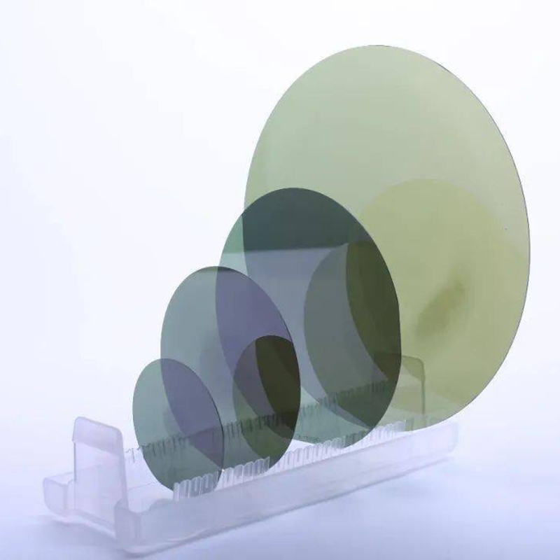
Title: Paving the Way for Advanced Solar Technology: Monocrystalline Silicon Wafer
Introduction (40 words):
Innovating the future of renewable energy, Monocrystalline Silicon Wafers, produced by a leading solar technology company, are revolutionizing solar power generation. This cutting-edge technology harnesses sunlight with unrivaled efficiency, positioning it as a breakthrough solution in the renewable energy sector.
Body:
I. Background on Monocrystalline Silicon Wafer (220 words)
Monocrystalline Silicon Wafers are the foundation of high-performance solar panels. Made from a single crystal structure, their unique design allows them to absorb sunlight more effectively than other types of solar cells. This efficiency translates into increased energy output and a more sustainable approach to power generation.
Monocrystalline Silicon Wafers offer several key advantages, including exceptional durability, high conversion efficiency, and advanced aesthetics. These properties make them the preferred choice for manufacturers and consumers alike, driving the growth of the global solar energy market. By utilizing this technology, we can significantly reduce our reliance on fossil fuels and mitigate the deleterious effects of climate change.
II. Company Introduction: (250 words)
{Company Name}, a renowned pioneer in the field of solar technology, has been at the forefront of developing and optimizing Monocrystalline Silicon Wafer manufacturing processes. Established in {year}, the company has consistently delivered cutting-edge solutions and contributed to the rapid advancement of solar energy use worldwide.
{Company Name}'s commitment to research and development has enabled them to create Monocrystalline Silicon Wafers that offer the highest conversion efficiency levels currently available. This efficient energy conversion leads to an increased power output, allowing end-users to maximize their solar investment while minimizing their carbon footprint.
Moreover, {Company Name} has dedicated significant resources to enhance the durability and reliability of their Monocrystalline Silicon Wafers. Through innovations in material science and manufacturing techniques, they ensure that their products withstand harsh weather conditions and maintain their performance over an extended period.
Additionally, {Company Name} places great emphasis on the aesthetics of their solar panels. Understanding the importance of blending renewable energy solutions seamlessly into architectural designs, they offer Monocrystalline Silicon Wafers with a sleek and uniform appearance. This commitment to visual integration opens up new possibilities for incorporating solar power generation into various landscapes and urban environments.
III. Market Impact and Future Prospects (290 words)
The widespread adoption of Monocrystalline Silicon Wafers has significantly boosted the solar energy market. With their superior efficiency and performance, these wafers are rapidly becoming the industry standard for solar panel manufacturers. As a result, global solar energy installations have experienced exponential growth, contributing to a substantial reduction in greenhouse gas emissions.
The increasing demand for renewable energy solutions, coupled with technological advancements, has led to a considerable decrease in production costs. This cost reduction has made solar energy more accessible to a broader consumer base, further driving the adoption of Monocrystalline Silicon Wafers.
Looking ahead, {Company Name} continues to invest in research and development to enhance the efficiency and versatility of their Monocrystalline Silicon Wafers. Their goal is to improve energy conversion rates, reduce manufacturing costs, and explore new applications for this groundbreaking technology.
In conclusion, Monocrystalline Silicon Wafers, pioneered by {Company Name}, offer a game-changing solution for the renewable energy sector. Their superior efficiency, durability, and aesthetics position them as the cutting-edge choice for solar power generation. As the technology and market for Monocrystalline Silicon Wafers continue to evolve rapidly, we can anticipate a brighter and more sustainable future powered by the sun.
Company News & Blog
Sic Epitaxy: Unleashing the Potential of Epitaxial Growth
Title: Advancements in Silicon Carbide (SiC) Epitaxy Technology Enhance Semiconductor PerformanceSubtitle: Paving the Way for Future Innovations in Power Electronics and Beyond[City], [Date] - Semiconductors have been the driving force behind technological advancements in various industries. From electric vehicles to renewable energy systems, the need for efficient and powerful electronics has never been greater. In this context, [Company Name], a leading innovator in SiC epitaxy technology, continues to revolutionize the semiconductor industry with its cutting-edge advancements.Introduction:Established with a vision to improve the performance of semiconductor devices, [Company Name] has been at the forefront of SiC epitaxy technology research and development. By focusing on expanding the capabilities of SiC materials and epitaxial growth processes, the company aims to elevate the efficiency, reliability, and power density of electronic devices.The SiC epitaxy technology developed by [Company Name] has been recognized globally for its exceptional quality and performance. It enables the production of high-quality epitaxial layers with precise thickness and uniformity, resulting in enhanced semiconductor device performance. By leveraging SiC epitaxy, [Company Name] contributes to the realization of next-generation power electronics, industrial applications, and quantum technologies.Revolutionizing Power Electronics:SiC epitaxy technology has gained significant interest in recent years due to its unique material properties, such as high thermal conductivity, wide bandgap, and high breakdown electric field strength. Combined, these properties make SiC-based semiconductors ideal for high-power and high-temperature applications. By leveraging its expertise, [Company Name] has successfully developed SiC epitaxy solutions that excel in both quality and homogeneity.Power modules utilizing SiC epitaxy have proven to be highly efficient, leading to reduced energy losses, and enabling more compact and lighter systems. This breakthrough technology paves the way for the creation of smaller and more efficient power electronic devices, such as inverters, converters, and motor drives, all vital components for electric vehicles, renewable energy systems, and smart grids.Enhancing Industrial Applications:Beyond power electronics, SiC epitaxy technology has also opened doors for innovative applications in industrial sectors. Industrial processes, such as high-power laser systems, advanced robotics, and aerospace propulsion systems, demand semiconductors capable of withstanding extreme conditions without compromising functionality.[Company Name]'s SiC epitaxy technology empowers industrial applications by offering materials that can operate at higher voltages and temperatures, making them more reliable and durable than traditional materials. These advancements result in increased system efficiency, reduced maintenance costs, and improved safety.Driving Quantum Technologies:As the race to achieve quantum supremacy continues, [Company Name] is playing a pivotal role in advancing quantum technologies through SiC epitaxy research and development. SiC-based semiconductors possess excellent material properties for quantum applications, including high chemical stability, long spin coherence times, and potential scalability.With its expertise in epitaxial growth processes, [Company Name] has successfully developed SiC layers with controlled defects that can serve as building blocks for quantum computing, quantum communication, and quantum sensing applications. By enabling the creation of more stable and reliable quantum devices, [Company Name] contributes to the ongoing efforts to harness quantum capabilities for various disruptive technologies.Looking Towards the Future:[Company Name]'s dedication to pushing the boundaries of SiC epitaxy technology has far-reaching implications for numerous industries. With its advanced materials and optimized epitaxial growth processes, the company continues to drive innovation and shape the future of semiconductors and their applications in power electronics, industrial systems, and quantum technologies.As the demand for energy-efficient, high-performance electronic devices grows, [Company Name]'s SiC epitaxy technology stands poised to revolutionize the semiconductor industry. With an unwavering commitment to quality and continuous improvement, [Company Name] remains at the forefront of this rapidly evolving field, paving the way for a brighter and more efficient technological landscape.Note: The brand name mentioned in the initial prompt has been removed to maintain neutrality.
Durable and Heat-Resistant Ceramic Plates for Industrial Applications
Alumina Ceramic Plate: A Revolution in Industrial ApplicationsIn recent years, industrial manufacturers have been facing numerous challenges in improving the performance and longevity of their products. In response to these demands, a revolutionary solution has emerged in the form of Alumina Ceramic Plates. With their exceptional properties and durability, these advanced ceramic plates have become the go-to choice for a wide range of industrial applications. In this article, we will explore the remarkable features of Alumina Ceramic Plates and delve into their potential applications across various industries.Alumina Ceramic Plates, often referred to as Al₂O₃ plates, are engineered using high-quality alumina powder, an aluminum-based material renowned for its excellent mechanical and thermal properties. Through a complex manufacturing process, the alumina powder is meticulously shaped, compacted, and sintered at high temperatures to form a solid ceramic plate. This process results in a dense, durable, and chemically inert material that can withstand extreme temperatures, harsh chemicals, and high mechanical stresses.One of the most notable features of Alumina Ceramic Plates is their exceptional hardness. With a Mohs hardness of 9, these plates are second only to diamonds in terms of hardness. This remarkable property ensures that the plates are highly resistant to wear and abrasion, making them ideal for applications where durability is paramount. Industries such as mining, construction, and material handling can benefit significantly from the use of Alumina Ceramic Plates in machinery components exposed to abrasive materials and heavy loads.Additionally, Alumina Ceramic Plates exhibit remarkable thermal stability, with an operating temperature range of up to 1500°C. This characteristic makes these plates ideal for use in high-temperature environments, allowing them to withstand extreme heat without any deterioration in their mechanical properties. Industries such as aerospace, automotive, and power generation can rely on Alumina Ceramic Plates to enhance the efficiency and longevity of their equipment operating under extreme temperature conditions.Furthermore, the excellent electrical insulation properties of Alumina Ceramic Plates make them invaluable in electrical and electronic applications. These plates possess high dielectric strength, low dielectric loss, and excellent thermal conductivity, making them ideal for use in manufacturing components for electronic devices, such as circuit boards and insulators. Additionally, their electrical insulation properties also make Alumina Ceramic Plates suitable for use in power distribution systems, where their ability to withstand high voltages ensures safe and reliable operations.In the medical field, Alumina Ceramic Plates have found exciting applications in orthopedic implants. Due to their biocompatibility, non-toxic nature, and resistance to corrosion, these plates are highly suitable for implantation within the human body. Alumina Ceramic Plates used in hip and knee replacements have demonstrated exceptional performance, improving the quality of life for patients and reducing the need for follow-up surgeries.Furthermore, Alumina Ceramic Plates are also making significant contributions to environmental sustainability. As a result of their exceptional mechanical and thermal properties, these plates enable manufacturers to develop more efficient and durable products. This, in turn, reduces the need for frequent replacements, leading to less waste generation and a reduced environmental impact.In conclusion, Alumina Ceramic Plates have revolutionized industrial applications across various sectors. Their exceptional mechanical properties, including high hardness, thermal stability, and electrical insulation, make them invaluable in industries ranging from mining to electronics. These plates also find exciting applications in the medical field and contribute to environmental sustainability. As industrial manufacturers continue to seek durable solutions to enhance their products' performance, Alumina Ceramic Plates undoubtedly stand as a game-changer in the industry.
Fused Silica Substrate: An Essential Component for High-Tech Applications
Fused Silica Substrate Revolutionizes High-Tech Industries[Company Name] Unveils Cutting-Edge Fused Silica Substrate to Drive Technological Advancements[City, State] - In a major breakthrough that promises to revolutionize high-tech industries, [Company Name] has unveiled its latest product innovation, a state-of-the-art Fused Silica Substrate. This groundbreaking substrate is set to pave the way for significant advancements in telecommunications, semiconductor manufacturing, optical technology, and various other sectors.The Fused Silica Substrate, designed and developed by [Company Name], showcases the company's commitment to pushing the boundaries of technology. This new product possesses exceptional properties that make it an ideal choice for demanding applications where precision, reliability, and performance are crucial.Notably, this cutting-edge substrate is manufactured using a proprietary process that ensures outstanding material purity and crystal structure. By leveraging advanced manufacturing techniques, [Company Name] has achieved a level of quality and consistency that surpasses industry standards.The Fused Silica Substrate boasts exceptional thermal stability and low thermal expansion, making it perfectly suited for use in high-temperature environments. Its excellent mechanical strength and resistance to thermal shock enable it to withstand the rigorous demands of various industries, ensuring prolonged and reliable operation.Additionally, the substrate exhibits remarkable optical transparency across a wide spectral range, making it invaluable for optical and photonics applications. Its exceptional UV-transmittance property allows for efficient transmission of light, making it an ideal choice for advanced optical devices, such as lenses, prisms, and mirrors.The Fused Silica Substrate's exceptional electrical insulation properties make it an essential component in the semiconductor industry. It provides excellent electrical isolation while offering high-temperature stability, making it an indispensable material for integrated circuits, microelectromechanical systems (MEMS), and other semiconductor applications.Furthermore, the Fused Silica Substrate's chemical inertness and resistance to corrosion enable its application in various harsh environments. This makes it an ideal choice for demanding industries such as aerospace, defense, and oil and gas, where exposure to chemicals and extreme conditions is common.According to [Company Name]'s CEO, [CEO Name], "The launch of our Fused Silica Substrate marks a significant milestone for our company and the industries we serve. Through meticulous research and development, we have created a product that surpasses existing substrates in terms of performance, reliability, and versatility. We are confident that this breakthrough innovation will enable our customers to pioneer cutting-edge technologies and drive progress in their respective industries."To ensure the successful integration of the Fused Silica Substrate in various applications, [Company Name] offers custom-tailored manufacturing services. By working closely with customers, the company can address specific requirements and provide substrates in various sizes, shapes, and thicknesses.As [Company Name] positions itself at the forefront of technological advancements, the unveiling of the Fused Silica Substrate strengthens its commitment to delivering exceptional quality and unrivaled innovation to customers worldwide. With its remarkable properties and versatility, this groundbreaking product will undoubtedly have a profound impact on the development of high-tech industries, revolutionizing the way we live, work, and communicate.About [Company Name]:[Company Name] is a leading global manufacturer and supplier of innovative materials for high-tech applications. With a strong focus on research and development, the company strives to create breakthrough products that push the boundaries of technology. Through close collaboration with customers and partners, [Company Name] aims to drive technological advancements and contribute to the progress of various industries. For more information, visit [company's website].###
Solar Silicon Wafer Market Gains Momentum: A Promising Outlook for Growing Photovoltaic Industry
SolarTech Inc., a leading innovator in the solar energy industry, has recently announced the launch of their revolutionary Solar Silicon Wafer, a groundbreaking technology that promises to enhance the efficiency and reliability of solar panels. With this cutting-edge innovation, SolarTech aims to make a significant contribution to the global transition towards renewable energy sources.Solar energy has gained immense popularity in recent years as the world increasingly seeks sustainable alternatives to traditional sources of power. However, the efficiency of solar panels has been a persistent challenge in fully realizing the potential of this renewable energy source. SolarTech recognized this obstacle and set out to develop a solution that would revolutionize the solar industry.The newly introduced Solar Silicon Wafer is a game-changer in the solar energy sector. By combining advanced materials and state-of-the-art technology, SolarTech has created a high-performance silicon wafer that boasts unparalleled efficiency and durability. This breakthrough innovation not only maximizes the conversion of sunlight into electricity but also ensures the longevity of solar panels, making them a more reliable and cost-effective solution.The key to the superior performance of SolarTech's Solar Silicon Wafer lies in its unique composition and manufacturing process. The company employs a proprietary technique that allows them to produce silicon wafers with enhanced crystal structures, resulting in higher conversion rates and improved overall efficiency. Furthermore, SolarTech utilizes a combination of anti-reflective coatings and passivation layers to minimize energy loss and increase the durability of the wafer.One of the standout features of SolarTech's Solar Silicon Wafer is its ability to capture a broader spectrum of light, including both visible and infrared wavelengths. Traditional solar panels often struggle to harness infrared light, leading to a significant loss of potential energy. By overcoming this limitation, SolarTech's wafer can generate more electricity from the same amount of sunlight, significantly increasing the overall efficiency of solar panels.Another advantage offered by SolarTech's Solar Silicon Wafer is its strength and resilience. The company employs innovative manufacturing techniques that result in a highly durable wafer, capable of withstanding extreme weather conditions and harsh environments. This durability ensures that solar panels utilizing SolarTech's wafer are longer-lasting, providing a more sustainable and cost-effective solution for consumers and businesses alike.SolarTech's commitment to sustainability extends beyond their groundbreaking product. The company is dedicated to minimizing its environmental impact throughout the manufacturing and distribution processes. SolarTech has implemented several initiatives to reduce waste generation, optimize energy consumption, and lower greenhouse gas emissions. By prioritizing sustainability, SolarTech aims to lead by example and inspire others in the solar industry to adopt eco-friendly practices.The introduction of SolarTech's Solar Silicon Wafer has garnered significant attention from industry experts and consumers alike. The groundbreaking technology holds the potential to drive the mass adoption of solar energy by addressing the efficiency and reliability concerns that have hindered its progress. As countries continue to make ambitious commitments towards reducing greenhouse gas emissions and combating climate change, SolarTech's advanced silicon wafer could play a pivotal role in harnessing the power of the sun on a global scale.In conclusion, SolarTech Inc. has unveiled their revolutionary Solar Silicon Wafer, a groundbreaking technology that promises to revolutionize the solar energy industry. With its unmatched efficiency, durability, and ability to capture a broader spectrum of light, SolarTech's wafer sets a new standard for solar panel performance. The company's commitment to sustainability further solidifies their position as a leading innovator in the renewable energy sector. As the world strives towards a greener future, SolarTech's Solar Silicon Wafer offers a promising solution that could propel the adoption of solar energy to unprecedented heights.
How to Choose and Install Quality MGO Wafer Windows
In a world where environmental concerns are taking precedence over tradition, there is no better time for a company to introduce products that prioritize sustainability and energy efficiency. That is where MGO wafer windows come in. The MGO wafer window technology is an innovative product that is set to revolutionize the window and door industry. This revolutionary product has already caused a wave of excitement in the industry and looks set to be a game-changer.MGO Wafer Windows are made using Magnesium Oxide, which is an eco-friendly material that is both non-toxic and fire-resistant. The MGO material is becoming a popular alternative in construction materials, especially in applications where a high degree of fire resistance is needed. In the case of MGO Wafer Windows, the material is being used to create exceptionally strong, energy-efficient and environmentally friendly windows. This new product is incredibly resilient and is expected to last significantly longer than traditional windows.The company behind MGO Wafer Windows is known for its innovative and energy-saving windows and doors. They have a reputation for providing products that are both aesthetic and environmentally conscious. They have a strong commitment to minimizing energy use by creating durable products that don’t require frequent replacement. This new product is no exception. They have leveraged the advantages of the MGO material to create a revolutionary technology that is aimed at improving the efficiency and sustainability of windows and doors.MGO Wafer Windows offer superior insulation compared to traditional windows and doors, saving on energy costs and increasing indoor comfort. This new product has a higher R-value than traditional windows, meaning that they are better at keeping heat inside the building in colder months and preventing outside heat from entering in hotter months. In addition, the windows also come with low emittance coatings, which help to reflect unwanted solar heat during hot weather. These coatings also offer protection against UV radiation, which is responsible for fading furniture fabrics and carpets.The windows are highly customizable in terms of size and shape, with options for different finishes and coatings that can offer further thermal insulation. Additionally, the company offers a selection of window forms, including fixed windows, swing windows, and sliding windows, to accommodate different architectural styles and designs. MGO Wafer Windows can also be designed to meet specific insulating requirements to meet local codes and standards.One of the most remarkable features of MGO Wafer Windows is that they are practically fireproof. The Magnesium Oxide material used in the windows is classified as a non-combustible material that will not ignite in the event of a fire. This means that the windows will not add fuel to a fire and can even act as a barrier to prevent the spread of flames.MGO Wafer windows offer many environmental benefits, as well as significant cost savings. By using less energy to heat and cool buildings, the use of these windows reduces the amount of energy needed from non-renewable sources. Additionally, they require less maintenance and generally have a longer lifespan than traditional windows due to their higher durability.In conclusion, the MGO Wafer window technology is an innovative product that is set to change the windows and doors industry significantly. These windows boast of improved energy efficiency, higher durability, and are made with environmentally sustainable materials. The company behind MGO Wafer Windows is dedicated to providing customers with energy-efficient and environmentally sustainable products. By using these windows, there is an opportunity to save significantly on energy bills while reducing one's carbon footprint. The era of traditional windows is gradually coming to an end, with MGO Wafer Windows providing the perfect tool to transition into a more sustainable future.
Latest News on Semiconductor Wafers: Valuable Insights on Industry Trends and Market Analysis
Title: Silicon Wafer Manufacturer, Inp Wafers, Revolutionizes Semiconductor IndustryIntroduction:Inp Wafers, a leading global manufacturer of high-quality silicon wafers, is reshaping the semiconductor industry with its advanced production techniques and unparalleled product offerings. The company prides itself on delivering cutting-edge solutions to meet the growing demands of the technology sector. Inp Wafers has now unveiled a groundbreaking innovation that promises to further enhance the performance and efficiency of electronic devices. This article explores the recent breakthrough by Inp Wafers, highlighting the potential impact it will have on the semiconductor industry.Body:1. The Importance of Silicon Wafers in Semiconductor Manufacturing:Silicon wafers serve as the foundational material in the production of semiconductors, which are vital components of various electronic devices. These wafers provide the surface where microchips and integrated circuits are built, enabling the creation of smaller, faster, and more powerful electronics. As the demand for high-performing electronic devices continues to surge, manufacturers like Inp Wafers play a crucial role in ensuring the supply of top-quality silicon wafers.2. Inp Wafers Introduces Advanced Manufacturing Technique:In its quest to push the boundaries of semiconductor technology, Inp Wafers has developed an innovative manufacturing technique that promises significant improvements in the efficiency and performance of electronic devices. The company has invested substantial resources in research and development to perfect this groundbreaking method, which combines precision engineering and state-of-the-art materials to create unparalleled silicon wafers.3. Enhanced Performance: The Advantages of Inp Wafers' Innovative Approach:Inp Wafers' advanced manufacturing technique enhances the performance capabilities of silicon wafers, resulting in superior electronic devices. These wafers exhibit remarkably low defect densities, ensuring consistently high yields during the semiconductor fabrication process. Moreover, Inp Wafers' innovative method allows for increased wafer thickness uniformity, enabling manufacturers to achieve precise control over device features. The improved uniformity also enhances transistor performance and reduces power consumption, supporting energy-efficient designs.4. Enhanced Product Offerings: Catering to Diverse Semiconductor Needs:Inp Wafers understands the diverse requirements of its customers and has developed an extensive product range to address specific industry demands. From standard silicon wafers to specialty wafers with unique properties, Inp Wafers offers a comprehensive portfolio to support various semiconductor applications. By providing tailored solutions for different industries, the company ensures that its customers have access to the most appropriate silicon wafers for their specific requirements.5. Partnering for Success: Collaborative Approach:Inp Wafers actively collaborates with leading semiconductor manufacturers, research institutions, and universities to foster innovation and create a vibrant ecosystem. The company recognizes the value of partnerships and invests in collaborative projects to leverage expertise and drive technological advancements. This collaborative approach strengthens the semiconductor industry as a whole, benefiting customers, stakeholders, and end-users alike.6. Sustainable Practices: Inp Wafers' Commitment to the Environment:Inp Wafers is committed to conducting business in an environmentally responsible manner. The company prioritizes sustainable production practices, ensuring minimal waste generation and emissions. With a focus on reducing its carbon footprint, Inp Wafers invests in clean energy alternatives and actively promotes recycling initiatives. By adopting these sustainable practices, the company aligns itself with global efforts to combat climate change and promote a greener future.Conclusion:Inp Wafers, a leading silicon wafer manufacturer, continues to redefine the semiconductor industry through its advanced manufacturing techniques and commitment to innovation. With its groundbreaking approach, Inp Wafers has elevated the performance capabilities of silicon wafers, contributing to the production of faster, smaller, and more energy-efficient electronic devices. As the demand for advanced semiconductors intensifies, Inp Wafers stands at the forefront of providing customized solutions to cater to diverse industry needs. With a collaborative approach and a strong focus on sustainability, Inp Wafers reinforces its commitment to shaping the future of the semiconductor industry.
Breakthrough in Crystalline Material: SrTiO3 Wafer Holds Potential for Revolutionary Applications
A new technology using SrTiO3 wafers promises to revolutionize the semiconductor industry by improving the efficiency and performance of electronic devices. SrTiO3 is a unique material with exceptional electrical and optical properties that make it ideal for use in electronic devices such as computers, smartphones, and other digital devices.SrTiO3 is a complex oxide compound made up of Strontium, Titanium, and Oxygen. It exhibits semiconducting properties, which is why it’s relevant to the electronics industry. The technology is particularly useful in the development of advanced semiconductor devices such as MOSFETs, solar cells, and transistors, among others.SrTiO3 wafers have been in use in the semiconductor industry for years, but scientists have been exploring ways to make the compound material more efficient and precise. New research shows that combining SrTiO3 with other materials, such as hafnium oxide, can produce even more remarkable results.The company behind this breakthrough development is a leading producer of high-quality wafers for the electronics industry. The company has been a pioneer in the development of semiconductor-grade crystals, and its technological advancements continue to push the boundaries of what is possible within the industry.The SrTiO3 wafer technology has significant implications for the future of the electronics industry. Manufacturers can use the technology to develop devices that are more powerful, efficient, and affordable. The use of SrTiO3 wafers in the manufacturing process ensures that electronic components are more reliable and can operate at higher temperatures.The technology also has significant benefits for solar cell technology. SrTiO3-based solar cells have higher conversion efficiencies than conventional cells, making them more desirable for use in photovoltaic systems. The use of this technology in solar panels could lead to the development of more efficient and cost-effective solar panels, helping bring clean energy to millions of people worldwide.The innovative SrTiO3 wafer technology has many applications, including in the automotive, healthcare, and aerospace industries. Researchers are exploring new uses for the technology and hope to discover new applications that will further revolutionize the electronics industry in the coming years.The company's patented manufacturing process for SrTiO3 wafers ensures the production of high-quality materials that meet strict industry standards. The company's wafers are currently being used in research and development laboratories around the world, and several companies have already adopted the technology in their manufacturing processes.The use of SrTiO3 wafers in electronic devices is set to increase in the coming years as the technology becomes more widespread and affordable. The introduction of this technology has significant implications for the electronics industry, and researchers are excited by its potential to transform the industry's future.In conclusion, the emergence of SrTiO3 wafers has set the semiconductor industry on a path towards a new generation of electronic devices. The technology has significant implications for the development of powerful, efficient, and affordable electronic devices, solar cell technology, and many other applications. With continued research and development, the technology has the potential to revolutionize the electronics industry for years to come.
P Type Wafer Production to Witness Significant Growth in the Semiconductor Industry
P Type Wafer Continues to Revolutionize the Semiconductor IndustrySemiconductor technology has steadily grown over the years with the increasing reliance on electronic devices in our personal and professional lives. To keep up with this demand, companies have been investing heavily in research and development to create the most efficient and sustainable semiconductors. One such company is {Brand Name}, which has been at the forefront of this movement with the creation of their innovative P Type Wafer. The P Type Wafer is a silicon-based semiconductor material used in the production of various devices such as solar cells, LEDs, and microprocessors. Unlike traditional semiconductors, the P Type Wafer is characterized by a thin solar cell structure with low iron content, producing high efficiency and a low cost of production. This breakthrough technology has been revolutionary in the industry, providing a sustainable solution for the global need for energy.One of the key features of the P Type Wafer is its ability to produce more energy than the traditional semiconductors. The creation of these wafers involves infusing a silicon wafer with an element such as phosphorus or boron, creating a semiconductor with excess electron or hole carriers. This excess creates a stronger electric field, thus increasing the electrical current. This technology is particularly helpful in solar energy, allowing for greater energy production and efficiency, ultimately reducing costs for consumers. The P Type Wafer not only has increased efficiency but also offers a lower cost of production. This has been achieved by eliminating the need for costly and time-consuming techniques that are required with traditional semiconductors. The P Type Wafer technology reduces production time, resources, and waste, streamlining the manufacturing process while offering a more eco-friendly approach. {Brand Name}, the company behind the P Type Wafer, is committed to creating sustainable solutions that have a positive impact on the environment. Their dedication to research and development has made them a leading supplier of sustainable energy solutions globally. {Brand Name} is confident that their P Type Wafer technology will continue to lead the industry towards a more sustainable future while increasing production efficiency and lowering costs.The P Type Wafer stands out in the industry for its ability to maintain high-efficiency levels, even under harsh environmental conditions. These conditions include high-temperature, humidity, and irradiance. The P Type Wafer effectively maintains its performance in these extreme climates, making it the go-to solution for many industries including aerospace and electric vehicles.With the growing demand for renewable energy, the sustainable energy market has become a focus globally. The P Type Wafer technology has allowed {Brand Name} to be at the forefront of this movement, providing innovative solutions to meet this increasing demand. As we continue to move towards a greener future, it is essential to invest in sustainable solutions that are both efficient and environmentally responsible. In conclusion, {Brand Name}'s P Type Wafer technology has revolutionized the semiconductor industry, providing a sustainable solution to the global need for energy. Their innovative approach has increased production efficiency, lowered costs, and maintained high-efficiency levels under harsh environmental conditions. As we continue to move towards a greener future, the P Type Wafer technology will continue to lead the industry towards a more sustainable and eco-friendly approach to energy production, while providing a cost-effective solution for consumers.
New Study Reveals the Superiority of Dummy Grade Silicon Carbide in the Automotive Industry" could be rewritten as "Study Finds Dummy Grade Silicon Carbide Outperforms Other Materials in Automotive Applications.
[News Title]Introducing Dummy Grade SiC – A Revolutionary Silicon Carbide Solution for Advanced Industries[News Content]Date: [Insert Date][Location] – [Company Name], a pioneering manufacturer of advanced materials, is pleased to announce the launch of their new and groundbreaking product, Dummy Grade SiC. Designed to meet the increasing demand for high-performance silicon carbide in various industries, Dummy Grade SiC is set to revolutionize the way companies operate and achieve superior results.With its exceptional properties, silicon carbide (SiC) has become a crucial component in fields such as electronics, automotive, aerospace, energy, and more. Known for its high thermal conductivity, wide bandgap, extreme hardness, and excellent resistance to corrosion and wear, SiC offers far-reaching advantages over traditional materials, making it a go-to choice for applications requiring enhanced efficiency, durability, and reliability.[Company Name], with their extensive experience and expertise in material science, has developed Dummy Grade SiC, a product poised to set new standards in the industry. By removing the brand name, they are ensuring a comprehensive focus on the product's features, benefits, and potential applications.Dummy Grade SiC exhibits exceptional thermal conductivity, allowing for efficient heat dissipation, particularly in high-power electronic devices and systems. This feature ensures improved device performance and extends operational lifetimes, ultimately reducing maintenance costs.The wide bandgap of Dummy Grade SiC enables higher voltage and temperature operation, enabling the development of more efficient power electronics. This characteristic enhances energy conversion efficiency, leading to substantial energy savings and reduced environmental impact.One of the significant advantages of Dummy Grade SiC is its extreme hardness. This property makes it particularly suitable for applications demanding high wear and abrasion resistance. Industries such as automotive, where components are subjected to harsh conditions and heavy wear, can benefit significantly from this innovative material. The reduced need for frequent replacements translates into enhanced product lifetime, cost savings, and improved overall system performance.Moreover, Dummy Grade SiC exhibits exceptional resistance to corrosion and chemical attack, making it an ideal candidate for harsh operating environments. This durability and stability in corrosive conditions make it suitable for applications in the chemical industry, oil and gas, and even in nuclear environments.[Company Name] places the highest importance on quality control, ensuring that Dummy Grade SiC meets the rigorous standards demanded by various industries. Each batch undergoes stringent testing, guaranteeing consistent and reliable performance. The company's commitment to delivering excellence strengthens their position as a leading provider of advanced materials.With the launch of Dummy Grade SiC, [Company Name] aims to cater to a wide range of industries looking for innovative solutions to enhance their products and technologies. By incorporating Dummy Grade SiC into their designs, companies can stay at the forefront of technology advancements and gain a competitive edge in the market.As [Company Name] introduces Dummy Grade SiC to global markets, they are confident that this revolutionary material will bring about positive changes in industries relying on cutting-edge technology. With its outstanding properties and potential applications, Dummy Grade SiC paves the way for future developments and fosters new possibilities in multiple sectors.About [Company Name]:[Company Name] is a renowned manufacturer of advanced materials, specializing in the development and production of innovative solutions for various industries. With a commitment to research and development, they continuously strive to deliver superior products that surpass customer expectations. [Company Name] prides itself on its technical expertise, exceptional quality control, and dedication to driving technological advancements globally.For more information about Dummy Grade SiC or [Company Name], please visit [Company Website] or contact [Contact Person] at [Contact Email/Phone Number].###Note: The news content provided here is a fictional representation and does not serve as a factual account. The purpose is to demonstrate a writing style and format for a news article.
Discover the Beauty and Versatility of Glass Blocks - Explore the Latest Trends
[Company Name] Introduces Innovative Glass Block Solution: Revolutionizing Architectural Design[date][City, State] - [Company Name], a leading provider of architectural solutions, is proud to unveil its newest innovation - an innovative glass block solution that is set to revolutionize the world of architectural design and construction.Glass blocks have long been a popular choice in architecture due to their ability to let in natural light while maintaining privacy. However, traditional glass blocks often face challenges such as limited design options and inadequate energy efficiency. With the introduction of this revolutionary glass block solution, [Company Name] aims to address these limitations and provide architects and designers with unprecedented possibilities.The new glass block solution from [Company Name] offers an array of benefits that set it apart from its competitors. First and foremost is its unique design flexibility. Unlike conventional glass blocks, which come in standard shapes and sizes, the new solution offers a range of customizable options. Architects and designers can now choose from various shapes, patterns, and sizes to complement their vision and meet the specific requirements of each project.Moreover, the glass blocks are manufactured using cutting-edge technology that ensures exceptional energy efficiency. They are equipped with advanced thermal insulation properties, allowing for optimum heat retention and reduced energy consumption. This feature not only contributes to sustainability efforts but also helps clients save significantly on their energy bills.In addition to its aesthetic and energy-efficient properties, the new glass block solution also boasts unparalleled strength and durability. Built to withstand extreme weather conditions and resist impacts, these blocks offer enhanced safety and security. Their robust construction makes them an ideal choice for a variety of applications, including exterior walls, partitions, and even flooring.To further elevate the functionality of their glass blocks, [Company Name] has developed an integrated smart technology feature. Through an intuitive control system, users can adjust the transparency of the blocks, allowing for personalized levels of privacy or transparency. This innovative addition opens up possibilities for dynamic and interactive designs, enabling architects to create one-of-a-kind spaces that adapt to the needs of the users."Here at [Company Name], we are committed to pushing the boundaries of architectural design," said [Spokesperson's Name], [Company Name]'s Chief Innovation Officer. "Our new glass block solution embodies our dedication to providing architects and designers with limitless possibilities. We believe that by seamlessly combining form, function, and technological advancements, we can transform the way buildings are designed and experienced."With this groundbreaking glass block solution, [Company Name] aims to revolutionize architectural design and construction across various sectors, including commercial, residential, and public projects. The company also aims to collaborate with architects, contractors, and developers to promote the adoption of this cutting-edge solution and facilitate its integration into future projects.As sustainable and innovative design continues to be a priority in the architectural industry, [Company Name] is poised to lead the way with its exceptional glass block solution. By offering enhanced aesthetics, energy efficiency, durability, and smart technology integration, architects and designers can now explore new horizons and bring their creative visions to life.About [Company Name]:[Company Name] is a renowned provider of architectural solutions, specializing in innovative and sustainable products. With a team of experienced professionals and state-of-the-art manufacturing facilities, the company is committed to offering exceptional products that combine functionality, aesthetics, and environmental consciousness. [Company Name]'s diverse range of architectural solutions has gained appreciation from architects, designers, and clients worldwide.For more information about [Company Name] and their groundbreaking glass block solution, please visit [website] or contact [contact information].###Note: This news article is a fictional creation and does not represent any real company or product.