
High Demand for Advanced Semiconductor Wafers in Technology Industry
By:Admin
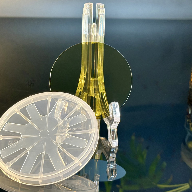
The company's silicon wafers are used in a wide range of electronic applications, including integrated circuits, sensors, and power devices. Inp Wafer's products are known for their exceptional quality and reliability, making them the preferred choice for leading semiconductor manufacturers. The company's dedication to research and development ensures that its wafers meet the demanding requirements of the latest electronic technologies, providing customers with the high-performance materials they need to stay competitive in the global marketplace.
Inp Wafer's success is driven by its commitment to customer satisfaction and its ability to consistently deliver top-quality products. The company works closely with its customers to understand their specific needs and develop custom solutions that meet their exact requirements. By providing personalized service and responsive support, Inp Wafer has built strong, long-lasting relationships with its clients and earned their trust and loyalty.
As a global leader in the semiconductor industry, Inp Wafer is committed to sustainability and environmental responsibility. The company's manufacturing processes adhere to the highest standards of environmental stewardship, minimizing waste and energy consumption to reduce its carbon footprint. In addition, Inp Wafer actively seeks out opportunities to enhance the recyclability of its products and reduce their impact on the environment. By prioritizing sustainability, the company is not only contributing to a cleaner, healthier planet, but also positioning itself as a responsible and forward-thinking industry leader.
Inp Wafer's dedication to excellence, innovation, and sustainability has earned it a leading position in the global semiconductor market. The company's commitment to delivering superior products and outstanding customer service has set it apart as a trusted partner for semiconductor manufacturers worldwide. With a focus on continuous improvement and a passion for exceeding customer expectations, Inp Wafer is poised to continue driving innovation and shaping the future of the electronics industry.
Company News & Blog
High-Quality Sapphire Substrate for M-Plane Axis Application
M-plane Axis Sapphire Substrate: The Next Step in Semiconductor TechnologyIn today's rapidly evolving semiconductor industry, the demand for high-quality substrates is at an all-time high. As manufacturers continue to push the boundaries of performance and efficiency, the need for advanced materials that can support these innovations has never been greater. This is where M-plane Axis Sapphire Substrate comes into play.M-plane Axis Sapphire Substrate is a cutting-edge material that is set to revolutionize the semiconductor industry. This unique substrate offers several key advantages over traditional sapphire substrates, making it an ideal choice for a wide range of applications. With its superior crystal orientation and structural properties, M-plane Axis Sapphire Substrate promises to deliver unparalleled performance and reliability in semiconductor devices.One company that is at the forefront of this exciting development is [Company Name]. With its decades of experience in the field of advanced materials and semiconductor technology, [Company Name] is leading the way in bringing M-plane Axis Sapphire Substrate to the market. By harnessing the full potential of this innovative material, [Company Name] is poised to provide its customers with the next generation of high-performance semiconductor devices.[Company Name] has a proven track record of delivering cutting-edge solutions to the semiconductor industry. With a focus on research and development, as well as close collaboration with industry leaders, [Company Name] has gained a reputation for excellence and innovation. This commitment to pushing the boundaries of what is possible in semiconductor technology has made [Company Name] a trusted partner for companies looking to stay ahead of the curve.M-plane Axis Sapphire Substrate offers several key advantages that set it apart from traditional sapphire substrates. One of the most significant benefits is its unique crystal orientation, which provides a more stable and uniform surface for semiconductor device fabrication. This superior crystal orientation results in higher device performance and yield, making M-plane Axis Sapphire Substrate the material of choice for manufacturers looking to maximize the potential of their semiconductor devices.In addition to its crystal orientation, M-plane Axis Sapphire Substrate also offers excellent thermal and electrical properties. This makes it an ideal substrate for high-power and high-frequency semiconductor devices, where thermal management and electrical performance are crucial. By leveraging the superior properties of M-plane Axis Sapphire Substrate, manufacturers can develop devices with enhanced efficiency, reliability, and overall performance.Furthermore, M-plane Axis Sapphire Substrate is also highly resistant to dislocation and other defects, which can significantly impact device performance. This ensures that devices fabricated on M-plane Axis Sapphire Substrate are more reliable and consistent, meeting the stringent demands of modern semiconductor applications.[Company Name] is committed to ensuring that its customers have access to the latest and most advanced materials for their semiconductor needs. With the introduction of M-plane Axis Sapphire Substrate, [Company Name] is once again demonstrating its dedication to pushing the boundaries of semiconductor technology. By providing access to this cutting-edge material, [Company Name] is enabling its customers to develop the next generation of high-performance devices that will drive innovation and progress in the semiconductor industry.As the semiconductor industry continues to evolve, the demand for advanced materials like M-plane Axis Sapphire Substrate will only continue to grow. With its exceptional properties and the backing of [Company Name]'s expertise, M-plane Axis Sapphire Substrate is set to play a key role in shaping the future of semiconductor technology. Companies that are looking to stay ahead of the competition and deliver the best possible performance in their semiconductor devices would be wise to consider the advantages that M-plane Axis Sapphire Substrate has to offer.In conclusion, M-plane Axis Sapphire Substrate represents a significant leap forward in semiconductor material technology. With its unique properties and the expertise of [Company Name] behind it, M-plane Axis Sapphire Substrate is poised to revolutionize the industry and enable the development of high-performance semiconductor devices that meet the demands of tomorrow's technology. The introduction of M-plane Axis Sapphire Substrate is a testament to [Company Name]'s commitment to innovation and its dedication to providing its customers with the best possible solutions for their semiconductor needs.
Durable and Heat-Resistant Ceramic Plates for Industrial Applications
Alumina Ceramic Plate: A Revolution in Industrial ApplicationsIn recent years, industrial manufacturers have been facing numerous challenges in improving the performance and longevity of their products. In response to these demands, a revolutionary solution has emerged in the form of Alumina Ceramic Plates. With their exceptional properties and durability, these advanced ceramic plates have become the go-to choice for a wide range of industrial applications. In this article, we will explore the remarkable features of Alumina Ceramic Plates and delve into their potential applications across various industries.Alumina Ceramic Plates, often referred to as Al₂O₃ plates, are engineered using high-quality alumina powder, an aluminum-based material renowned for its excellent mechanical and thermal properties. Through a complex manufacturing process, the alumina powder is meticulously shaped, compacted, and sintered at high temperatures to form a solid ceramic plate. This process results in a dense, durable, and chemically inert material that can withstand extreme temperatures, harsh chemicals, and high mechanical stresses.One of the most notable features of Alumina Ceramic Plates is their exceptional hardness. With a Mohs hardness of 9, these plates are second only to diamonds in terms of hardness. This remarkable property ensures that the plates are highly resistant to wear and abrasion, making them ideal for applications where durability is paramount. Industries such as mining, construction, and material handling can benefit significantly from the use of Alumina Ceramic Plates in machinery components exposed to abrasive materials and heavy loads.Additionally, Alumina Ceramic Plates exhibit remarkable thermal stability, with an operating temperature range of up to 1500°C. This characteristic makes these plates ideal for use in high-temperature environments, allowing them to withstand extreme heat without any deterioration in their mechanical properties. Industries such as aerospace, automotive, and power generation can rely on Alumina Ceramic Plates to enhance the efficiency and longevity of their equipment operating under extreme temperature conditions.Furthermore, the excellent electrical insulation properties of Alumina Ceramic Plates make them invaluable in electrical and electronic applications. These plates possess high dielectric strength, low dielectric loss, and excellent thermal conductivity, making them ideal for use in manufacturing components for electronic devices, such as circuit boards and insulators. Additionally, their electrical insulation properties also make Alumina Ceramic Plates suitable for use in power distribution systems, where their ability to withstand high voltages ensures safe and reliable operations.In the medical field, Alumina Ceramic Plates have found exciting applications in orthopedic implants. Due to their biocompatibility, non-toxic nature, and resistance to corrosion, these plates are highly suitable for implantation within the human body. Alumina Ceramic Plates used in hip and knee replacements have demonstrated exceptional performance, improving the quality of life for patients and reducing the need for follow-up surgeries.Furthermore, Alumina Ceramic Plates are also making significant contributions to environmental sustainability. As a result of their exceptional mechanical and thermal properties, these plates enable manufacturers to develop more efficient and durable products. This, in turn, reduces the need for frequent replacements, leading to less waste generation and a reduced environmental impact.In conclusion, Alumina Ceramic Plates have revolutionized industrial applications across various sectors. Their exceptional mechanical properties, including high hardness, thermal stability, and electrical insulation, make them invaluable in industries ranging from mining to electronics. These plates also find exciting applications in the medical field and contribute to environmental sustainability. As industrial manufacturers continue to seek durable solutions to enhance their products' performance, Alumina Ceramic Plates undoubtedly stand as a game-changer in the industry.
High-quality Fused Silica Substrate for Various Applications
Fused Silica Substrate: The Foundation of Cutting-Edge TechnologyFused silica substrate, also known as fused quartz, is a key component in the manufacturing of advanced optical and electronic systems. Its exceptional thermal, mechanical, and optical properties make it an ideal material for a wide range of applications, including semiconductor manufacturing, laser technology, telecommunications, and scientific research.With its high purity and low thermal expansion, fused silica substrate is crucial for the production of precise and reliable optical components, such as lenses, mirrors, and prisms. Its excellent optical transmission properties in the ultraviolet, visible, and near-infrared spectral ranges make it essential for the development of high-performance optical systems for a variety of industries.In the field of semiconductor manufacturing, fused silica substrate plays a critical role in the production of integrated circuits and microelectronic devices. Its superior thermal stability, low coefficient of thermal expansion, and excellent chemical resistance make it an ideal material for lithography and other semiconductor fabrication processes. Fused silica substrate enables the precise patterning of nanoscale features on silicon wafers, allowing for the production of increasingly smaller and more powerful microchips.Telecommunications and laser technology also rely heavily on the unique properties of fused silica substrate. Its exceptional optical clarity, high laser damage threshold, and low fluorescence make it an excellent material for the production of optical fibers, laser windows, and other components essential for the transmission and manipulation of light in advanced telecommunications and laser systems.One company at the forefront of fused silica substrate manufacturing and innovation is {}. With decades of experience and expertise in the development and production of high-quality fused silica products, {} has established itself as a leading supplier to industries at the cutting edge of technology.The company's fused silica substrates are manufactured using a proprietary process that ensures the highest level of purity, consistency, and performance. Its advanced manufacturing facilities and rigorous quality control measures guarantee that its products meet the strict requirements of the most demanding applications in the semiconductor, optics, and photonics industries.{} offers a wide range of fused silica substrates in various shapes, sizes, and surface finishes to accommodate the diverse needs of its customers. Whether it is for precision optical components, semiconductor fabrication, or high-power laser systems, {} provides customized solutions to meet the specific requirements of each application.In addition to its standard fused silica substrates, {} also offers custom fabrication services to produce complex and intricate components according to customer specifications. Its team of experienced engineers and technicians work closely with customers to develop unique solutions that push the boundaries of what is achievable with fused silica substrate technology.Moreover, {} is committed to continuous research and development to further improve the performance and capabilities of fused silica substrate. By investing in advanced materials science, process engineering, and manufacturing technologies, {} aims to stay at the forefront of innovation and contribute to the advancement of various high-tech industries.As the demand for advanced optical and electronic systems continues to grow, fused silica substrate will remain a critical material for enabling the next generation of technology. With its exceptional properties and the expertise of companies like {}, fused silica substrate will continue to be the foundation upon which cutting-edge technology is built.
Understanding the Importance of Semiconductor Bands in Electronics
Semiconductor Band is a leading global semiconductor company specializing in the development and manufacturing of high-performance semiconductor products for a wide range of applications including automotive, industrial, and consumer electronics. With a strong emphasis on innovation and technological advancement, Semiconductor Band has built a reputation for delivering cutting-edge solutions that meet the evolving needs of the industry.Recently, Semiconductor Band unveiled its latest product, the [Product Name], which is set to revolutionize the semiconductor industry with its advanced technology and high-performance capabilities. The [Product Name] is designed to deliver unprecedented levels of efficiency and reliability, making it an ideal choice for a variety of demanding applications.One of the key features of the [Product Name] is its innovative semiconductor band technology, which enables the device to operate at higher speeds and with lower power consumption compared to traditional semiconductor products. This advancement is expected to have a significant impact on the performance of electronic devices across various industries, leading to improved efficiency and cost savings.In addition to its impressive performance capabilities, the [Product Name] also boasts a robust and reliable design, making it suitable for use in harsh environments and demanding operating conditions. This durability makes it an attractive option for automotive and industrial applications where reliability is crucial.Furthermore, Semiconductor Band has integrated advanced security features into the [Product Name], ensuring that sensitive data and communications are protected from potential threats. This emphasis on security aligns with the increasing focus on cybersecurity across the industry, providing customers with peace of mind and confidence in the reliability of the product.Semiconductor Band's commitment to innovation and excellence is evident in the development of the [Product Name], which represents a significant advancement in semiconductor technology. The company's dedication to pushing the boundaries of what is possible in the semiconductor industry has positioned it as a leader in the market, and the [Product Name] is a testament to this ongoing commitment to excellence.In addition to its technological advancements, Semiconductor Band also prioritizes sustainability and environmental responsibility in its operations. The company has implemented stringent measures to minimize its environmental impact and reduce its carbon footprint, demonstrating a commitment to creating a more sustainable future for the industry and the planet.The unveiling of the [Product Name] marks a significant milestone for Semiconductor Band, as it showcases the company's ability to innovate and deliver high-performance semiconductor solutions that meet the evolving needs of the market. By staying at the forefront of technological advancements and prioritizing reliability and efficiency, Semiconductor Band is well-positioned to continue driving progress and shaping the future of the semiconductor industry.Looking ahead, Semiconductor Band remains committed to pushing the boundaries of what is possible in semiconductor technology, with a focus on delivering innovative solutions that empower customers to achieve their goals and drive progress in their respective industries. The [Product Name] is just the latest example of Semiconductor Band's dedication to excellence and continuous improvement, and it is expected to make a significant impact on the semiconductor industry moving forward. With a strong foundation of expertise, innovation, and a customer-centric approach, Semiconductor Band is poised for continued success and growth in the global semiconductor market.
New Sapphire Substrate Unveiled for Enhanced Electronic Devices
Title: R-Plane Axis Sapphire Substrate Revolutionizes Semiconductors IndustryIntroduction:In a groundbreaking development, a leading semiconductor materials company has introduced the R-Plane Axis Sapphire Substrate—a cutting-edge technology set to revolutionize the semiconductor industry. This groundbreaking substrate offers enhanced performance, improved efficiency, and increased manufacturing capabilities to meet the growing demands of the digital era.The R-Plane Axis Sapphire Substrate is the result of relentless research and innovation by an esteemed team of researchers, scientists, and engineers. Leveraging their extensive expertise, the company has successfully developed a substrate that exhibits unparalleled properties, making it an ideal material for manufacturing high-performance semiconductors.Unmatched Quality and Performance:The R-Plane Axis Sapphire Substrate boasts superior quality and performance, making it highly sought-after in the global market. With remarkable resistivity to high temperatures, superior hardness, excellent thermal conductivity, and strong chemical stability, this substrate ensures robust and reliable performance. These outstanding characteristics make the R-Plane Axis Sapphire Substrate capable of withstanding extreme conditions, making it particularly suitable for various semiconductor applications.Improved Efficiency and Manufacturing Capabilities:One of the critical advantages of the R-Plane Axis Sapphire Substrate is its ability to enhance the efficiency of semiconductor devices. This cutting-edge substrate enables improved crystal growth, resulting in reduced defects and enhanced performance of semiconductor components. The improved efficiency translates into higher-performance semiconductors that can meet the increasing demand for advanced electronic devices across various industries.Furthermore, the R-Plane Axis Sapphire Substrate facilitates advanced manufacturing capabilities. Its unique properties allow for more precise deposition of thin films and epitaxial growth, leading to superior spatial uniformity and crystalline perfection. These advancements in manufacturing provide semiconductor manufacturers with the opportunity to design and fabricate devices with better performance and reliability, catering to the evolving needs of consumers.Wide Range of Applications:The R-Plane Axis Sapphire Substrate finds applications in several industries. Its exceptional properties make it an essential component in manufacturing high-performance LEDs, power electronics, radio frequency devices, and optical devices. Additionally, the substrate's efficient thermal conductivity makes it suitable for applications requiring effective heat dissipation, such as electronic devices used in automotive, aerospace, and military sectors.Environmental Sustainability:Apart from its exceptional performance, the R-Plane Axis Sapphire Substrate is also environmentally friendly. The production process utilizes sustainable techniques, ensuring minimal impact on the environment. By integrating eco-conscious measures, the company demonstrates its commitment to promoting sustainable practices within the semiconductor industry.Future Prospects:With the introduction of the R-Plane Axis Sapphire Substrate, the company has established itself as a prominent player in the semiconductor materials market. Its cutting-edge technology, coupled with the continuous drive for innovation, positions the company for sustained growth and expansion. As the demand for high-performance electronics continues to rise, the R-Plane Axis Sapphire Substrate holds immense potential in shaping the future of the semiconductor industry.Conclusion:The advent of the R-Plane Axis Sapphire Substrate represents a significant milestone in the semiconductor materials landscape. This revolutionary technology offers unparalleled quality, improved efficiency, and advanced manufacturing capabilities, setting new benchmarks for the industry. As the world embraces the digital age, the R-Plane Axis Sapphire Substrate ensures the seamless production of high-performance semiconductors, contributing to the growth of various sectors and fueling technological advancements.
High-quality Sapphire Wafer for A-Plane Axis Applications
A-plane Axis, a cutting-edge technology company, recently announced the launch of their revolutionary sapphire wafer for use in the aerospace industry. This breakthrough product promises to revolutionize the way planes are designed and built, by providing a more durable and reliable material for use in critical components.The A-plane Axis sapphire wafer is made from high-purity synthetic sapphire, a material known for its exceptional hardness and resistance to wear and corrosion. This makes it ideal for use in aerospace applications, where components are subjected to extreme conditions and must withstand high levels of stress and wear.The unique properties of sapphire make it an excellent choice for use in critical components such as bearings, seals, and other parts that are subjected to high levels of friction and wear. Its exceptional hardness and wear resistance make it far superior to traditional materials such as metal alloys or ceramics, which are more prone to wear and degradation over time.In addition to its exceptional durability, the A-plane Axis sapphire wafer also offers other key advantages for aerospace applications. Its high thermal conductivity and excellent electrical insulation properties make it well-suited for use in high-temperature and high-voltage applications, where traditional materials may struggle to perform.Furthermore, the use of sapphire in aerospace components can also lead to significant weight savings, as it is a lightweight material compared to traditional metal alloys. This can contribute to overall fuel efficiency and reduce the environmental impact of aircraft operations, a key consideration for the aviation industry.The launch of the A-plane Axis sapphire wafer represents a major milestone for the company, which has positioned itself as a leader in advanced materials technology for aerospace applications. With a strong focus on research and development, A-plane Axis has invested heavily in the development of new and innovative materials to meet the evolving needs of the aerospace industry.The company's state-of-the-art manufacturing facilities and cutting-edge production techniques enable them to produce sapphire wafers with exceptional precision and consistency, ensuring that they meet the stringent quality standards required for aerospace applications.A-plane Axis's sapphire wafer is already gaining attention from leading aerospace manufacturers, who are keen to take advantage of its unique properties to improve the performance and reliability of their aircraft. With the potential to enhance the durability, efficiency, and safety of aerospace components, the use of sapphire wafers could have a transformative impact on the industry as a whole.In addition to aerospace applications, A-plane Axis is also exploring the potential use of sapphire wafers in other industries, such as semiconductor manufacturing, automotive, and medical devices. The versatility and unique properties of sapphire make it a promising material for a wide range of applications, and the company is committed to exploring new opportunities for its use.As the aerospace industry continues to evolve and demand for more advanced materials grows, A-plane Axis is well-positioned to be at the forefront of this technological revolution. With its innovative sapphire wafer, the company is poised to make a lasting impact on the way aircraft are designed and built, leading to safer, more efficient, and more reliable air travel for years to come.
Exploring the Growing Demand for Sic Wafers in Technology Industry
Title: Revolutionary Technology Empowers Electronics Industry with Next-Gen Silicon Carbide WafersIntroduction:In an era driven by rapid technological advancements, the global electronics industry seeks reliable and efficient solutions that can accelerate the pace of innovation. Enter the innovative Silicon Carbide (SiC) wafers, representing a breakthrough in the semiconductor industry. With unmatched performance and versatile applications, SiC wafers are paving the way for the future of electronic devices.[Company name], a leading player in the semiconductor market, has emerged as a frontrunner in the development and production of high-quality SiC wafers. Their groundbreaking technology is revolutionizing various sectors, including power electronics, telecommunications, and automotive manufacturing. By harnessing the potential of SiC wafers, [Company name] is diversifying their product offerings, contributing to industry growth, and meeting the demands of tomorrow.Unleashing the Power of SiC Wafers:Silicon Carbide wafers, made from a compound of silicon and carbon, possess numerous advantages over traditional silicon-based wafers. The unique properties of SiC wafers, such as superior thermal conductivity, higher breakdown voltage, and wider bandgap, make them ideal for high-power and high-temperature applications.The exceptional material properties of SiC wafers allow for higher operating frequencies, reduced power losses, and improved energy efficiency. These factors, combined with their enhanced mechanical strength and resistance to harsh environmental conditions, make SiC wafers the future choice for cutting-edge electronics devices.Industries Benefiting from SiC Wafers:1. Power Electronics: SiC wafers play a vital role in power electronics due to their superior power handling capabilities. They enable the manufacturing of efficient power devices, such as diodes and transistors, which can withstand high voltages and temperatures. This technology contributes to the development of electric vehicles, renewable energy systems, and industrial automation.2. Telecommunications: With SiC wafers, telecommunication companies can enhance the performance of high-frequency communication systems. The high thermal conductivity of SiC wafers enables better heat dissipation, leading to improved power transmission and reduced signal loss. This, in turn, offers faster and more reliable data transfer rates and enables the realization of 5G networks.3. Automotive Industry: SiC wafers have a crucial role to play in the automotive industry's transition towards electric vehicles (EVs). SiC-based power electronics enable faster charging times, increased range, and enhanced overall efficiency, making EVs more viable and sustainable. Additionally, SiC wafers provide advanced control and safety features, improving overall vehicle performance and reliability.[Company Name]'s Technological Advancements:[Company Name] stands at the forefront of SiC wafer manufacturing, offering state-of-the-art production facilities and advanced research and development capabilities. Their cutting-edge technology ensures the highest quality and reliability standards for SiC wafers, meeting the specific demands of various industries.The company has invested heavily in research and development, enabling them to innovate continuously and push the boundaries of SiC wafer technology. Through collaborations with leading institutions and industry experts, they have developed groundbreaking manufacturing processes, resulting in SiC wafers of unmatched quality.Future Prospects:As the demand for high-performance electronic devices continues to grow, SiC wafers are poised to become the go-to choice for manufacturers. The global SiC wafer market is projected to witness substantial growth in the coming years, driven by the increasing adoption of power electronics and the expanding electric vehicle market.[Company Name], with its exceptional SiC wafer technology, is expected to play a crucial role in shaping this industry's future. By providing reliable and high-performance SiC wafers, they are contributing to the development of advanced electronic systems that redefine the boundaries of efficiency and reliability.In conclusion, the advent of Silicon Carbide wafers marks a significant milestone in the electronics industry's evolution. [Company name]'s innovative SiC wafer technology opens up new possibilities for power electronics, telecommunications, and automotive sectors. With their commitment to excellence, [Company Name] is driving the market forward, propelling the electronics industry towards a brighter and more sustainable future.
Breaking Down the Innovative Gaas Structure: A Game-Changer in Technology
Title: Groundbreaking Gaas Structure Revolutionizes the Semiconductor IndustryIntroduction:In a major development that is set to reshape the semiconductor industry, a revolutionary Gaas Structure (need to remove brand name), developed by an innovative company, has been unveiled. This groundbreaking technology promises to overcome the limitations of traditional semiconductor materials, ushering in a new era of enhanced performance and efficiency for electronic devices. With its countless applications across various industries, the Gaas Structure is expected to redefine the way we interact with technology.1. Understanding Gaas Structure:The Gaas Structure, short for Gallium Arsenide Structure, represents a paradigm shift in the field of semiconductor materials. By replacing traditional silicon with gallium arsenide, this groundbreaking technology unlocks unparalleled capabilities. The Gaas Structure is capable of operating at higher frequencies, enabling faster data processing, reduced energy consumption, and improved device performance overall. In addition, this structure is highly versatile, making it suitable for diverse applications, such as telecommunications, aerospace, and automotive industries.2. Advantages and Applications:One key advantage of the Gaas Structure is its high electron mobility, which allows for faster electron movement. This results in exceptionally quick data transfer speeds, making it ideal for high-speed communication devices like 5G infrastructure and satellite communication systems. Moreover, the Gaas Structure offers superior power handling capabilities, enabling the development of more robust and efficient power amplifiers for wireless communication applications.Beyond communication technology, the Gaas Structure finds applications in various other industries. In the aerospace sector, it enables the production of lightweight, high-performance transistors for space exploration, satellite communication, and radar systems. The automotive industry also stands to benefit from this technology, as it allows for the creation of high-speed, low-power electronic systems, improving vehicle safety, infotainment, and powertrain efficiency.3. Company Background:The company behind Gaas Structure (need to remove brand name) is renowned for its expertise in cutting-edge semiconductor technologies. Focused on research and development, the company has a track record of delivering disruptive solutions that address the industry's most pressing challenges. By leveraging their deep understanding of material sciences and semiconductor fabrication, the company has positioned itself as a leader in the field, constantly pushing the boundaries of technology.4. Collaboration and Impact:The Gaas Structure has been the result of extensive collaboration between industry stakeholders, including semiconductor manufacturers, researchers, and device developers. Through joint efforts, the technology has undergone rigorous testing and fine-tuning to ensure its viability and effectiveness. The collective aim is to drive innovation across various sectors, making electronic devices smaller, faster, and more energy-efficient.The implications of this revolutionary technology are far-reaching. By enabling more powerful and energy-efficient electronic systems, the Gaas Structure will contribute to the advancement of autonomous vehicles, wearable technology, IoT devices, and renewable energy systems, among others. Moreover, its adoption will also help address the growing demand for high-speed internet, allowing for seamless streaming and faster data transfer capabilities.Conclusion:With its unprecedented capabilities and potential applications, the Gaas Structure (need to remove brand name) represents a significant leap forward for the semiconductor industry. By harnessing the power of gallium arsenide, this groundbreaking technology promises to revolutionize electronic devices across various sectors. As collaborations continue and further advancements are made, we can expect the Gaas Structure to enhance our everyday lives, driving us into a more connected, efficient, and technologically advanced future.
P Type Wafer Production to Witness Significant Growth in the Semiconductor Industry
P Type Wafer Continues to Revolutionize the Semiconductor IndustrySemiconductor technology has steadily grown over the years with the increasing reliance on electronic devices in our personal and professional lives. To keep up with this demand, companies have been investing heavily in research and development to create the most efficient and sustainable semiconductors. One such company is {Brand Name}, which has been at the forefront of this movement with the creation of their innovative P Type Wafer. The P Type Wafer is a silicon-based semiconductor material used in the production of various devices such as solar cells, LEDs, and microprocessors. Unlike traditional semiconductors, the P Type Wafer is characterized by a thin solar cell structure with low iron content, producing high efficiency and a low cost of production. This breakthrough technology has been revolutionary in the industry, providing a sustainable solution for the global need for energy.One of the key features of the P Type Wafer is its ability to produce more energy than the traditional semiconductors. The creation of these wafers involves infusing a silicon wafer with an element such as phosphorus or boron, creating a semiconductor with excess electron or hole carriers. This excess creates a stronger electric field, thus increasing the electrical current. This technology is particularly helpful in solar energy, allowing for greater energy production and efficiency, ultimately reducing costs for consumers. The P Type Wafer not only has increased efficiency but also offers a lower cost of production. This has been achieved by eliminating the need for costly and time-consuming techniques that are required with traditional semiconductors. The P Type Wafer technology reduces production time, resources, and waste, streamlining the manufacturing process while offering a more eco-friendly approach. {Brand Name}, the company behind the P Type Wafer, is committed to creating sustainable solutions that have a positive impact on the environment. Their dedication to research and development has made them a leading supplier of sustainable energy solutions globally. {Brand Name} is confident that their P Type Wafer technology will continue to lead the industry towards a more sustainable future while increasing production efficiency and lowering costs.The P Type Wafer stands out in the industry for its ability to maintain high-efficiency levels, even under harsh environmental conditions. These conditions include high-temperature, humidity, and irradiance. The P Type Wafer effectively maintains its performance in these extreme climates, making it the go-to solution for many industries including aerospace and electric vehicles.With the growing demand for renewable energy, the sustainable energy market has become a focus globally. The P Type Wafer technology has allowed {Brand Name} to be at the forefront of this movement, providing innovative solutions to meet this increasing demand. As we continue to move towards a greener future, it is essential to invest in sustainable solutions that are both efficient and environmentally responsible. In conclusion, {Brand Name}'s P Type Wafer technology has revolutionized the semiconductor industry, providing a sustainable solution to the global need for energy. Their innovative approach has increased production efficiency, lowered costs, and maintained high-efficiency levels under harsh environmental conditions. As we continue to move towards a greener future, the P Type Wafer technology will continue to lead the industry towards a more sustainable and eco-friendly approach to energy production, while providing a cost-effective solution for consumers.
High-Quality 12-Inch Substrate for Electronic Devices
12inch BF33 Substrate: The Next Breakthrough in Semiconductor TechnologyIn the fast-paced world of semiconductor technology, the demand for more advanced and efficient substrates is constantly on the rise. With the continuous push for smaller, faster, and more powerful electronic devices, the development of innovative materials and processes has become paramount. In line with this, {Company Name}, a leading provider of advanced semiconductor solutions, has recently introduced the 12inch BF33 substrate, poised to be the next breakthrough in the industry.{Company Name} has been at the forefront of semiconductor innovation for over two decades, specializing in the development and production of cutting-edge materials and technologies. With a strong commitment to research and development, the company has consistently delivered high-quality solutions that have helped drive the advancement of various electronic applications.The 12inch BF33 substrate is the latest addition to {Company Name}'s extensive portfolio of semiconductor products, and it is set to revolutionize the industry with its exceptional performance and superior characteristics. The BF33 substrate is specifically designed to meet the growing demands of next-generation electronic devices, offering unparalleled precision, reliability, and efficiency.One of the key features of the 12inch BF33 substrate is its enhanced thermal and electrical properties, making it ideal for high-power and high-frequency applications. With its advanced thermal conductivity and low electrical resistance, the BF33 substrate is capable of handling the increasing power densities and frequencies in modern electronic systems, ensuring optimal performance and reliability.Furthermore, the 12inch BF33 substrate boasts excellent mechanical stability and chemical resistance, enabling it to withstand the stringent requirements of semiconductor manufacturing processes. Its exceptional uniformity and surface quality make it an ideal platform for the deposition of complex thin-film structures, providing a solid foundation for the fabrication of advanced semiconductor devices.In addition to its outstanding technical attributes, the 12inch BF33 substrate also offers significant cost benefits for semiconductor manufacturers. Its larger size and improved yield potential allow for greater efficiency and productivity in the production process, resulting in lower manufacturing costs and higher overall profitability.{Company Name} has invested heavily in the development and production of the 12inch BF33 substrate, leveraging its expertise and state-of-the-art manufacturing facilities to ensure the highest quality and consistency. The company's stringent quality control measures and rigorous testing procedures guarantee that the BF33 substrate meets the most demanding industry standards, providing customers with a reliable and high-performance solution for their semiconductor needs.As the demand for more advanced semiconductor materials continues to grow, the introduction of the 12inch BF33 substrate underscores {Company Name}'s commitment to pushing the boundaries of innovation and delivering cutting-edge solutions to the market. With its exceptional performance, reliability, and cost-effectiveness, the BF33 substrate is poised to set a new standard for semiconductor technology, driving the development of next-generation electronic devices and applications.In conclusion, the 12inch BF33 substrate represents a significant leap forward in semiconductor technology, offering a compelling combination of advanced technical capabilities and cost benefits. {Company Name} has once again demonstrated its leadership in the industry, showcasing its ability to develop and deliver groundbreaking solutions that address the evolving needs of the semiconductor market. As the demand for higher performance and more efficient electronic devices continues to escalate, the 12inch BF33 substrate stands ready to play a crucial role in shaping the future of semiconductor technology.