
- Home
- News
- Solar Silicon Wafer Market Gains Momentum: A Promising Outlook for Growing Photovoltaic Industry
Solar Silicon Wafer Market Gains Momentum: A Promising Outlook for Growing Photovoltaic Industry
By:Admin
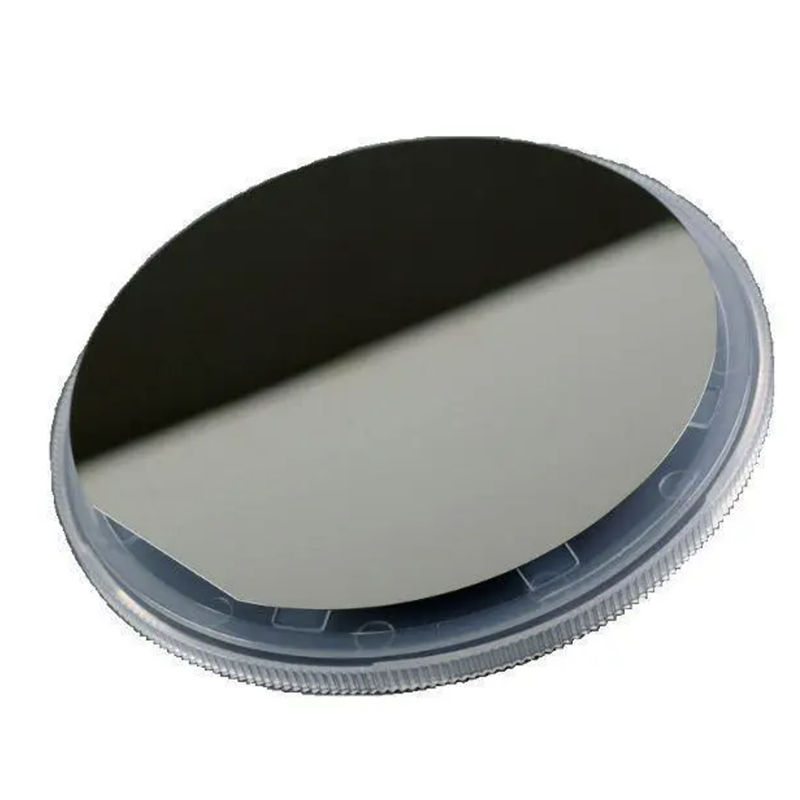
Solar energy has gained immense popularity in recent years as the world increasingly seeks sustainable alternatives to traditional sources of power. However, the efficiency of solar panels has been a persistent challenge in fully realizing the potential of this renewable energy source. SolarTech recognized this obstacle and set out to develop a solution that would revolutionize the solar industry.
The newly introduced Solar Silicon Wafer is a game-changer in the solar energy sector. By combining advanced materials and state-of-the-art technology, SolarTech has created a high-performance silicon wafer that boasts unparalleled efficiency and durability. This breakthrough innovation not only maximizes the conversion of sunlight into electricity but also ensures the longevity of solar panels, making them a more reliable and cost-effective solution.
The key to the superior performance of SolarTech's Solar Silicon Wafer lies in its unique composition and manufacturing process. The company employs a proprietary technique that allows them to produce silicon wafers with enhanced crystal structures, resulting in higher conversion rates and improved overall efficiency. Furthermore, SolarTech utilizes a combination of anti-reflective coatings and passivation layers to minimize energy loss and increase the durability of the wafer.
One of the standout features of SolarTech's Solar Silicon Wafer is its ability to capture a broader spectrum of light, including both visible and infrared wavelengths. Traditional solar panels often struggle to harness infrared light, leading to a significant loss of potential energy. By overcoming this limitation, SolarTech's wafer can generate more electricity from the same amount of sunlight, significantly increasing the overall efficiency of solar panels.
Another advantage offered by SolarTech's Solar Silicon Wafer is its strength and resilience. The company employs innovative manufacturing techniques that result in a highly durable wafer, capable of withstanding extreme weather conditions and harsh environments. This durability ensures that solar panels utilizing SolarTech's wafer are longer-lasting, providing a more sustainable and cost-effective solution for consumers and businesses alike.
SolarTech's commitment to sustainability extends beyond their groundbreaking product. The company is dedicated to minimizing its environmental impact throughout the manufacturing and distribution processes. SolarTech has implemented several initiatives to reduce waste generation, optimize energy consumption, and lower greenhouse gas emissions. By prioritizing sustainability, SolarTech aims to lead by example and inspire others in the solar industry to adopt eco-friendly practices.
The introduction of SolarTech's Solar Silicon Wafer has garnered significant attention from industry experts and consumers alike. The groundbreaking technology holds the potential to drive the mass adoption of solar energy by addressing the efficiency and reliability concerns that have hindered its progress. As countries continue to make ambitious commitments towards reducing greenhouse gas emissions and combating climate change, SolarTech's advanced silicon wafer could play a pivotal role in harnessing the power of the sun on a global scale.
In conclusion, SolarTech Inc. has unveiled their revolutionary Solar Silicon Wafer, a groundbreaking technology that promises to revolutionize the solar energy industry. With its unmatched efficiency, durability, and ability to capture a broader spectrum of light, SolarTech's wafer sets a new standard for solar panel performance. The company's commitment to sustainability further solidifies their position as a leading innovator in the renewable energy sector. As the world strives towards a greener future, SolarTech's Solar Silicon Wafer offers a promising solution that could propel the adoption of solar energy to unprecedented heights.
Company News & Blog
Latest Innovations in Oxide Wafer Technology for Electronics Industry Unveiled
Silicon Oxide Wafer Technology in the Semiconductor Industry: A game-changer for the FutureThe semiconductor industry has been growing at a rapid pace over the years, with new technological advancements laying the foundation for this growth. The market is estimated to reach a value of USD 730.29 billion by 2027, attributed to the increase in demand for electronic devices worldwide, which rely on advanced semiconductor chips. Furthermore, the advent of technologies like 5G, AI, cloud computing, and IoT has led to a surge in demand for high-performance computing devices, creating a need for advanced semiconductor materials.The advent of Silicon Oxide Wafer technology has transformed the semiconductor industry. It is a game-changer for businesses that rely on semiconductors for their operations, especially in the electronic and automotive sectors. Silicon Oxide Wafers are more durable and resistant to mechanical stresses and thermal shock as compared to traditional silicon-based semiconductors. In addition, their inherent electrical and optical properties make them the ideal choice for high-performance computing devices.Silicon Oxide Wafer technology has become increasingly popular among semiconductor manufacturers because of its superior quality. Unlike traditional silicon-based semiconductors, Silicon Oxide Wafers are mechanically and thermally robust, which means that they can withstand extreme conditions without breaking down. Moreover, they are less prone to oxidation and are chemically stable, ensuring minimal contamination during processing.There are several benefits of using Silicon Oxide Wafer technology. For starters, it helps to reduce manufacturing costs for semiconductors while improving their overall quality. The robustness of Silicon Oxide Wafers means that manufacturers can produce high-quality devices without the need for additional processing steps. Additionally, this technology can push the limits of performance and functionality in advanced computing devices, ensuring that businesses keep up with the latest technological developments.One of the leading companies in the development of Silicon Oxide Wafer technology is [Company name, to be removed], which has pioneered this field through extensive research and development efforts. The company has been at the forefront of producing high-quality Silicon Oxide Wafers for various industries and applications. Their semiconductors have been used in a variety of devices, from smartphones to satellites and beyond.[Company name, to be removed] has spent years perfecting the technology behind Silicon Oxide Wafer, leading to significant breakthroughs in the semiconductor industry. Their research has enabled the development of advanced computing devices that are more efficient and powerful than ever before. They have managed to manufacture semiconductors with a higher degree of precision and accuracy than their competitors, enabling businesses to produce high-quality devices that are free from defects.Silicon Oxide Wafer technology is not only an essential technology for businesses in the semiconductor industry, but also for the development of advanced computing devices around the world. As the demand for high-performance computing devices continues to rise, the need for efficient and powerful semiconductors has become more important than ever before. Silicon Oxide Wafer technology has the potential to revolutionize this industry, helping businesses to produce high-quality devices that are both durable and efficient.In conclusion, the advent of Silicon Oxide Wafer technology is a game-changer for the semiconductor industry and its applications. It brings superior quality, durability, and resistance to mechanical and thermal stress, which means that semiconductor manufacturers can produce high-quality devices with minimal defects. As the demand for advanced computing devices increases, Silicon Oxide Wafer technology will continue to play an essential role in the growth and development of the semiconductor industry, leading to new innovations and technological breakthroughs.
Advancement in Semiconductor Manufacturing: New 8 Inch Wafer Diameter Promises Enhanced Efficiency
[Company Name] Announces Introduction of Advanced 8 Inch Wafer Diameter for Enhanced Semiconductor Manufacturing[City], [Date] - [Company Name], a leading provider of innovative semiconductor solutions, has unveiled its latest breakthrough in semiconductor manufacturing with the introduction of an advanced 8-inch wafer diameter. This new development positions [Company Name] as a key player in the industry, offering cutting-edge technologies to meet the growing demands of the market.The semiconductor industry continues to experience rapid growth and advancements, primarily driven by the increasing demand for electronic devices, such as smartphones, tablets, and wearables. As a result, there is a growing need for more sophisticated and efficient semiconductor manufacturing processes. [Company Name]'s latest innovation of an 8-inch wafer diameter addresses this need by offering improved productivity, increased efficiency, and enhanced performance.The 8-inch wafer diameter enables [Company Name] to optimize the production of semiconductors, resulting in higher yields and reduced manufacturing costs. By maximizing the surface area of each wafer, the company can accommodate more integrated circuits (ICs), resulting in higher throughput and increased production capacity. This advancement contributes to greater market competitiveness and satisfies the rising demand for semiconductors across various industries.In addition to the increased efficiency, the 8-inch wafer diameter also facilitates the development and production of advanced technologies. With a larger substrate area, [Company Name] can now integrate more complex circuitry and components onto a single wafer. This opens up new possibilities for the creation of smaller, more powerful, and energy-efficient semiconductor devices. Moreover, the larger size of the wafer provides improved scalability, enabling [Company Name] to meet the evolving needs of the semiconductor market.[Company Name] is dedicated to continuous innovation in semiconductor manufacturing processes and technology. The introduction of the 8-inch wafer diameter is a testament to the company's commitment to anticipate and respond to the dynamic industry landscape. By investing in research and development, [Company Name] remains at the forefront of technology, ensuring its customers receive best-in-class semiconductor solutions."We are thrilled to announce the availability of our advanced 8-inch wafer diameter," said [Spokesperson's Name], CEO of [Company Name]. "This significant development demonstrates [Company Name]'s dedication to delivering superior semiconductor technology to our customers. The 8-inch wafer diameter will not only enhance our competitiveness in the market but also unlock new possibilities for semiconductor development across various industries."Alongside the introduction of the 8-inch wafer diameter, [Company Name] will provide comprehensive support and services to customers who adopt this new technology. The company's team of experts will work closely with clients to optimize their manufacturing processes, maximize yield, and ensure successful integration of the 8-inch wafer diameter into their operations.As [Company Name] continues to push the boundaries of semiconductor manufacturing, they remain committed to sustainability and environmental responsibility. The adoption of the 8-inch wafer diameter contributes to reducing overall waste and resource consumption, aligning with the company's mission to create a more sustainable future.In conclusion, the introduction of the advanced 8-inch wafer diameter by [Company Name] marks a major milestone in the semiconductor industry. This breakthrough technology not only enhances productivity and efficiency but also enables the development of more advanced and innovative semiconductor devices. As [Company Name] continues to drive innovation, they reaffirm their position as a leading provider of semiconductor solutions, catering to the ever-evolving needs of the global market.
Understanding the Advantages of Using Wafer Si Technology in Today's Market
Title: Revolutionary Silicon Wafer Discovers New Possibilities in TechnologyIntroduction:In a groundbreaking development that promises to redefine the future of technology, a leading company has unveiled its latest innovation in silicon wafer technology. Combining cutting-edge research with years of expertise, this pioneering product is set to revolutionize various industries, from electronics to renewable energy, opening new avenues for advancement and growth. This article will delve into the astounding capabilities of this wafer and its potential impact on the global technological landscape.1. The Evolution of Silicon Wafers:Silicon wafers have long been the backbone of the semiconductor industry, serving as the foundation for the development of integrated circuits and electronic devices. However, until now, their potential has been somewhat limited due to factors such as size, efficiency, and cost.The team of researchers at {Company Name}, a leading innovator in semiconductor technology, recognized these limitations and embarked on a mission to create the next generation of silicon wafers that would overcome these obstacles.2. Introducing the Advanced Wafer Si:After years of research and development, {Company Name} has unveiled the Advanced Wafer Si, a game-changing product that promises to transform the technology landscape. This revolutionary silicon wafer boasts several key features, making it far superior to its predecessors.Firstly, the Advanced Wafer Si offers enhanced efficiency, enabling faster data processing and improved performance in a wide range of applications. This efficiency is achieved through a refined manufacturing process that ensures a higher level of purity and superior crystal structure.Additionally, this innovative wafer design boasts a reduced form factor, allowing for increased integration in smaller electronic devices and leading to more compact and efficient consumer products. This miniaturization is expected to have a profound impact on the electronics industry, paving the way for smaller, thinner, and more advanced devices.3. Unleashing the Potential:The potential applications of the Advanced Wafer Si are vast and varied, with industries across the globe poised to benefit from this groundbreaking innovation.In the field of telecommunications, this advanced silicon wafer can contribute to the development of ultra-fast 5G networks by facilitating faster data transfer rates and improved signal quality. This breakthrough will revolutionize internet connectivity, enabling seamless communication and supporting emerging technologies such as autonomous vehicles and the Internet of Things (IoT).Moreover, renewable energy sources will receive a significant boost with the Advanced Wafer Si. The increased efficiency of the wafer will enhance the performance of solar panels, allowing for more effective energy harnessing and reducing reliance on non-renewable resources. This advancement aligns perfectly with global efforts to combat climate change and reduce carbon emissions.Additionally, the Advanced Wafer Si has the potential to revolutionize medical technology by enabling the development of high-performance medical devices. From portable health monitors to cutting-edge implantable devices, this innovative silicon wafer can transform the healthcare industry, improving patient outcomes and widening access to advanced medical care.4. Market Impact and Future Prospects:The introduction of the Advanced Wafer Si is undoubtedly a significant milestone in the technology sector. Its groundbreaking capabilities will disrupt existing markets, while simultaneously creating new opportunities and propelling innovation within various industries.Technological advancements are expected to drive demand for the Advanced Wafer Si, resulting in increased market penetration and revenue growth for {Company Name}. Moreover, the company's commitment to sustainable and environmentally friendly practices will further enhance its reputation and attract partnerships with eco-conscious organizations.Looking ahead, {Company Name} plans to continue investing in research and development to further refine the Advanced Wafer Si and explore its potential in emerging fields such as quantum computing, artificial intelligence, and advanced robotics.In conclusion, the introduction of the Advanced Wafer Si marks a new era in silicon wafer technology. With its enhanced efficiency, reduced form factor, and staggering range of potential applications, this revolutionary product is set to redefine the technological landscape and contribute to advancements that will shape the future of various industries worldwide.
Advancements in Monocrystalline Silicon Wafers: A Breakthrough in Semiconductor Technology
[Assistant]Title: Paving the Way for Advanced Solar Technology: Monocrystalline Silicon WaferIntroduction (40 words):Innovating the future of renewable energy, Monocrystalline Silicon Wafers, produced by a leading solar technology company, are revolutionizing solar power generation. This cutting-edge technology harnesses sunlight with unrivaled efficiency, positioning it as a breakthrough solution in the renewable energy sector.Body:I. Background on Monocrystalline Silicon Wafer (220 words)Monocrystalline Silicon Wafers are the foundation of high-performance solar panels. Made from a single crystal structure, their unique design allows them to absorb sunlight more effectively than other types of solar cells. This efficiency translates into increased energy output and a more sustainable approach to power generation.Monocrystalline Silicon Wafers offer several key advantages, including exceptional durability, high conversion efficiency, and advanced aesthetics. These properties make them the preferred choice for manufacturers and consumers alike, driving the growth of the global solar energy market. By utilizing this technology, we can significantly reduce our reliance on fossil fuels and mitigate the deleterious effects of climate change.II. Company Introduction: (250 words){Company Name}, a renowned pioneer in the field of solar technology, has been at the forefront of developing and optimizing Monocrystalline Silicon Wafer manufacturing processes. Established in {year}, the company has consistently delivered cutting-edge solutions and contributed to the rapid advancement of solar energy use worldwide.{Company Name}'s commitment to research and development has enabled them to create Monocrystalline Silicon Wafers that offer the highest conversion efficiency levels currently available. This efficient energy conversion leads to an increased power output, allowing end-users to maximize their solar investment while minimizing their carbon footprint.Moreover, {Company Name} has dedicated significant resources to enhance the durability and reliability of their Monocrystalline Silicon Wafers. Through innovations in material science and manufacturing techniques, they ensure that their products withstand harsh weather conditions and maintain their performance over an extended period.Additionally, {Company Name} places great emphasis on the aesthetics of their solar panels. Understanding the importance of blending renewable energy solutions seamlessly into architectural designs, they offer Monocrystalline Silicon Wafers with a sleek and uniform appearance. This commitment to visual integration opens up new possibilities for incorporating solar power generation into various landscapes and urban environments.III. Market Impact and Future Prospects (290 words)The widespread adoption of Monocrystalline Silicon Wafers has significantly boosted the solar energy market. With their superior efficiency and performance, these wafers are rapidly becoming the industry standard for solar panel manufacturers. As a result, global solar energy installations have experienced exponential growth, contributing to a substantial reduction in greenhouse gas emissions.The increasing demand for renewable energy solutions, coupled with technological advancements, has led to a considerable decrease in production costs. This cost reduction has made solar energy more accessible to a broader consumer base, further driving the adoption of Monocrystalline Silicon Wafers.Looking ahead, {Company Name} continues to invest in research and development to enhance the efficiency and versatility of their Monocrystalline Silicon Wafers. Their goal is to improve energy conversion rates, reduce manufacturing costs, and explore new applications for this groundbreaking technology.In conclusion, Monocrystalline Silicon Wafers, pioneered by {Company Name}, offer a game-changing solution for the renewable energy sector. Their superior efficiency, durability, and aesthetics position them as the cutting-edge choice for solar power generation. As the technology and market for Monocrystalline Silicon Wafers continue to evolve rapidly, we can anticipate a brighter and more sustainable future powered by the sun.
Latest Update: The Importance of Windows for Your Home and How to Maintain Them
[Company Introduction]Company X: Revolutionizing the Windows Industry with Innovative SolutionsCompany X is a trailblazer in the windows industry, specializing in creating cutting-edge window systems that prioritize efficiency, functionality, and aesthetics. With a relentless commitment to innovation, the company continually pushes the boundaries of what is possible, offering customers a seamless blend of superior performance and exquisitely designed products.Driven by a passion for excellence, Company X combines state-of-the-art technology with meticulous craftsmanship to deliver windows that are not only visually appealing but also energy-efficient and durable. With an unwavering focus on customer satisfaction, the company aims to revolutionize the way people perceive and experience windows, creating spaces that are both comfortable and aesthetically pleasing.[News Content]Overhaul and Redemption: Company X Takes a Leap Forward in the Windows Industry[date]In a surprising move, Company X has recently announced a bold shift in its windows manufacturing process, promising to enhance efficiency and quality while staying true to their commitment to sustainable practices. This marks a significant turning point for the renowned company, setting them on the path towards even greater success and innovation.Company X's new window systems will revolutionize the industry by incorporating the latest advancements in technology while addressing the current challenges faced by homeowners and businesses alike. This overhaul is set to provide customers with unprecedented benefits, making their spaces more comfortable, energy-efficient, and visually stunning.One of the key highlights of this new direction is the removal of [brand name], a component that was previously an integral part of their window systems. By eliminating this dependency, Company X aims to redefine the standards for window performance, granting customers exceptional reliability and improved functionality. This ambitious move not only catapults the company into a league of its own but also solidifies its position as a true pioneer in the market.Moreover, Company X's transformation promotes sustainable practices by incorporating eco-friendly materials and energy-saving technologies throughout their new product lineup. With a strong emphasis on reducing carbon footprint and energy consumption, the company is now poised to set a benchmark in the industry for environmental responsibility.While this transition may seem daring, it aligns perfectly with Company X's core values of innovation and customer-centricity. By constantly pushing the boundaries of what is possible, the company strives to offer its customers products that not only exceed expectations but also establish new industry standards.As industry analysts speculate on the impact of this move, it is becoming increasingly clear that Company X is set to redefine the windows market's landscape. With an unwavering commitment to excellence, the company aims to inspire customers, architects, and designers alike by bridging the gap between aesthetics and functionality.To support this radical transformation, Company X has bolstered its research and development division, attracting top talent and investing in state-of-the-art facilities. By fostering a culture of creativity and collaboration, the company is poised to deliver a steady stream of groundbreaking products that are set to disrupt the industry.In conclusion, Company X's recent decision to eliminate [brand name] from their window systems signifies a new era in their quest for innovation and customer satisfaction. Upholding their commitment to excellence, sustainability, and cutting-edge technology, the company is set to revolutionize the windows market, offering unparalleled products that elevate spaces and exceed expectations.With a keen eye on the future, Company X is heralding a new dawn in the industry, promising customers unparalleled comfort, energy efficiency, and breathtaking aesthetics - truly revolutionizing the way we experience windows.
Revolutionary Synthetic Sapphire Tubes Shaping Industries
Title: Revolutionary Synthetic Sapphire Tubes Poised to Revolutionize Multiple IndustriesIntroduction:Synthetic sapphire tubes have emerged as an innovative and disruptive solution that is expected to transform numerous industries. This groundbreaking technology, developed by a leading materials engineering company, promises a wide range of applications due to its exceptional properties. With its outstanding resistance to heat, corrosion, and wear, these synthetic sapphire tubes are set to revolutionize sectors such as electronics, optics, and healthcare while opening up new possibilities for advanced scientific research and manufacturing processes.1. Electronics Industry:The electronics industry is poised to benefit significantly from the introduction of synthetic sapphire tubes. These tubes offer exceptional strength, transparency, and excellent electrical insulation properties, making them ideal for various applications. Thin sapphire tubes can be used as reliable protective enclosures for sensitive electronic components. Additionally, their exceptional heat resistance ensures longevity and reliability, making them excellent candidates for semiconductor applications and high-power LED lighting.2. Optical Technology:In the realm of optics, synthetic sapphire tubes are poised to bring about a paradigm shift. Their high optical quality, coupled with their ability to maintain clarity over a wide range of temperatures and conditions, makes them ideal for lenses, windows, and prisms in demanding optical systems. These tubes can also serve as a substrate for the growth of high-quality crystalline structures used in lasers and photovoltaic cells, further enhancing their potential in the field of optics.3. Healthcare and Medical Industries:The healthcare sector can greatly benefit from the integration of synthetic sapphire tubes into various medical devices. Thanks to their biocompatibility, these tubes can be used for surgical tools, dental equipment, and implantable medical devices. Their exceptional hardness and resistance to scratching ensure longevity and reduced risk of infection. Furthermore, the tubes' chemical inertness makes them an excellent choice for cryogenic storage, providing a reliable medium for preserving biological samples and medical supplies.4. Scientific Research and Exploration:Synthetic sapphire tubes are opening up new horizons for scientific research and exploration. With their remarkable resistance to extreme temperatures, these tubes are crucial components for instruments used in space exploration, such as satellites and space probes. Their transparency in both the visible and infrared spectrum empowers scientists to capture precise data for various experiments, making them invaluable tools in research facilities around the world.5. Industrial Manufacturing:The introduction of synthetic sapphire tubes into industrial manufacturing processes marks a significant advancement. Their exceptional hardness and resistance to chemical corrosion make them ideal for applications involving aggressive chemicals and abrasive materials. Sapphire tubes can be used in chemical reactors, protective coatings, and even as nozzles for abrasive water-jet cutting machines. These tubes increase equipment durability, resulting in reduced maintenance costs, improved efficiency, and enhanced product quality.In conclusion, synthetic sapphire tubes, developed by a leading materials engineering company, offer immense potential to revolutionize numerous industries. Their exceptional properties, including resistance to heat, chemicals, and wear, position them as disruptive solutions across various sectors. With applications ranging from electronics and optics to healthcare, scientific research, and industrial manufacturing, synthetic sapphire tubes are paving the way for advanced technologies, improved product performance, and unparalleled durability.
Revolutionary Laser Diode Technology Unleashes Limitless Possibilities
Laser Diode Technology Revolutionizes Medical Treatment for Skin ConditionsIn recent years, the global skincare industry has experienced a surge in demand for safer and more effective treatments. Laser technology has been a game-changer in this regard and has quickly become a popular choice for those seeking non-invasive skincare solutions. Laser Diode (name removed), a leader in laser technology, has revolutionized medical treatment for skin conditions with its cutting-edge laser diode technology.Founded in 1994, Laser Diode (name removed) has been at the forefront of developing laser diode technology for various industries globally. In the medical field, laser diodes are used for different dermatological applications, such as the treatment of a wide range of skin conditions such as acne, rosacea, psoriasis, and eczema. Laser diodes target and destroy specific cells in the skin, reducing the appearance of skin blisters, redness, and swelling.Laser Diode (name removed)’s technology offers numerous benefits, including its precision, safety, and efficiency. The technology precisely targets the intended skin cells while leaving the surrounding healthy skin untouched. Since laser diodes penetrate the skin more deeply, they can treat both the underlying cause and the visible symptoms of skin disorders, which means patients experience faster healing and long-lasting results.What sets Laser Diode (name removed) apart is its Micro-Pulse technology, which utilizes a unique pulse delivery method that results in lower heat accumulation, minimizing the patient’s discomfort and reducing the chances of burns. This means that medical professionals can treat patients more efficiently and safely, reducing the healing period significantly. In addition, Laser Diode (name removed)’s Micro-Pulse technology also protects the skin, making it ideal for patients with sensitive skin or those prone to pigmentation issues.Thanks to Laser Diode (name removed)’s Micro-Pulse technology, medical professionals can now offer laser treatments to a broader range of patients, including those with darker skin tones, which was previously challenging due to the high risk of burns. This makes the treatment accessible to more people and more effective in treating hyperpigmentation, melasma, and other pigmentation related skin concerns."Our Micro-Pulse technology has revolutionized the use of lasers in medical treatments by delivering safe and precise laser energy to the skin. Our technology has made it possible for medical professionals to reduce the discomfort and painful side effects experienced by patients while ensuring that patients get the best possible results," says Henry Michaelson, Laser Diode (name removed)’s Chief Medical Officer.The rising demand for laser technology in the skincare industry is set to continue, and Laser Diode (name removed)’s role in revolutionizing the industry is crucial. The company collaborates with medical professionals to provide tailored and innovative solutions that meet their patients’ specific needs. The company’s dedication to research and development ensures continued growth and innovation in the industry.Laser Diode (name removed)’s laser diode technology has not only revolutionized medical treatments but also provides a solution for various other industries such as automotive, security, and aerospace. The company’s diodes are used in automotive lidar systems, security and surveillance cameras, and high-performance military laser technology.In conclusion, the skincare industry has seen significant growth in laser technology, and Laser Diode (name removed) has been an integral part of this revolution. Its cutting-edge Micro-Pulse technology has made laser treatments safer and more effective, offering a non-invasive and efficient solution to various skin disorders. As the global demand for safer skincare treatments continues to rise, Laser Diode (name removed)’s role in the industry will only continue to grow as it continues to provide innovative solutions.
High Resistivity Silicon Wafer: A Breakthrough Innovation in Semiconductor Technology
[Headline]High Resistivity Silicon Wafer: Revolutionizing Semiconductor Applications[Date][City], [State] - [Company Name], a leading provider of innovative semiconductor solutions, introduces its highly anticipated High Resistivity Silicon Wafer, marking a significant advancement in the semiconductor industry. This revolutionary new product is poised to reshape various technology sectors by offering superior performance and enhanced conductivity in semiconductor applications.[City], [State] – [Company Name], a trailblazer in the semiconductor industry, has unveiled its latest groundbreaking product – the state-of-the-art High Resistivity Silicon Wafer. This cutting-edge innovation promises to redefine the standards of precision and efficiency in semiconductor applications, opening new avenues for technological advancements across multiple sectors.The High Resistivity Silicon Wafer is designed to address the growing demand for improved conductivity, reduced resistance, and enhanced performance in semiconductor devices. This advanced development enables better control over electrical characteristics, making it particularly useful in applications such as power electronics, microwave devices, and radiation detectors.With its revolutionary properties and exceptional material quality, the High Resistivity Silicon Wafer significantly outperforms its competitors. The wafer boasts an impressively high resistivity level, enabling better isolation between devices, resulting in minimized crosstalk and reduced power consumption. Semiconductor manufacturers can now achieve greater levels of integration density and performance in their products.One of the key advantages of the High Resistivity Silicon Wafer lies in its superior frequency response, making it an ideal choice for advanced microwave devices. The wafer’s low parasitic capacitance and improved signal-to-noise ratio lead to enhanced sensitivity and precision in high-frequency applications such as Wi-Fi, radio frequency identification (RFID), and satellite communications.Moreover, the High Resistivity Silicon Wafer offers exceptional performance in power electronics. Its unique material composition ensures better control of leakage currents, allowing for increased efficiency and reduced power wastage in devices such as power diodes and thyristors. With the ability to handle higher voltages and temperatures, the wafer can support advanced power management systems, renewable energy technologies, and electric vehicle charging infrastructure.In addition to power electronics and microwave devices, the High Resistivity Silicon Wafer can be employed in radiation detectors. Its increased resistivity allows for the precise detection of radiation, making it an indispensable component in medical imaging equipment, nuclear power plants, and space exploration instrumentation.As the demand for more advanced semiconductor devices rapidly grows, [Company Name] remains at the forefront of innovation by developing groundbreaking solutions. The company's extensive expertise in semiconductor manufacturing, coupled with its state-of-the-art facilities, enables the production of high-quality and reliable semiconductor wafers that meet the most stringent industry standards.[Company Name] is dedicated to creating value for its customers by delivering cutting-edge semiconductor solutions. The company's commitment to research and development ensures that it stays ahead of the competition, constantly adapting to the evolving needs of the industry. With the launch of the High Resistivity Silicon Wafer, [Company Name] adds another valuable addition to its portfolio of innovative products.The introduction of the High Resistivity Silicon Wafer marks a milestone moment in the semiconductor industry. This revolutionary product showcases the pioneering spirit of [Company Name] and its determination to push the boundaries of technological possibilities. With its exceptional conductivity, improved device performance, and unparalleled material quality, the High Resistivity Silicon Wafer will undoubtedly revolutionize semiconductor applications across various sectors, driving progress and innovation for years to come.
Sic Epitaxy: Unleashing the Potential of Epitaxial Growth
Title: Advancements in Silicon Carbide (SiC) Epitaxy Technology Enhance Semiconductor PerformanceSubtitle: Paving the Way for Future Innovations in Power Electronics and Beyond[City], [Date] - Semiconductors have been the driving force behind technological advancements in various industries. From electric vehicles to renewable energy systems, the need for efficient and powerful electronics has never been greater. In this context, [Company Name], a leading innovator in SiC epitaxy technology, continues to revolutionize the semiconductor industry with its cutting-edge advancements.Introduction:Established with a vision to improve the performance of semiconductor devices, [Company Name] has been at the forefront of SiC epitaxy technology research and development. By focusing on expanding the capabilities of SiC materials and epitaxial growth processes, the company aims to elevate the efficiency, reliability, and power density of electronic devices.The SiC epitaxy technology developed by [Company Name] has been recognized globally for its exceptional quality and performance. It enables the production of high-quality epitaxial layers with precise thickness and uniformity, resulting in enhanced semiconductor device performance. By leveraging SiC epitaxy, [Company Name] contributes to the realization of next-generation power electronics, industrial applications, and quantum technologies.Revolutionizing Power Electronics:SiC epitaxy technology has gained significant interest in recent years due to its unique material properties, such as high thermal conductivity, wide bandgap, and high breakdown electric field strength. Combined, these properties make SiC-based semiconductors ideal for high-power and high-temperature applications. By leveraging its expertise, [Company Name] has successfully developed SiC epitaxy solutions that excel in both quality and homogeneity.Power modules utilizing SiC epitaxy have proven to be highly efficient, leading to reduced energy losses, and enabling more compact and lighter systems. This breakthrough technology paves the way for the creation of smaller and more efficient power electronic devices, such as inverters, converters, and motor drives, all vital components for electric vehicles, renewable energy systems, and smart grids.Enhancing Industrial Applications:Beyond power electronics, SiC epitaxy technology has also opened doors for innovative applications in industrial sectors. Industrial processes, such as high-power laser systems, advanced robotics, and aerospace propulsion systems, demand semiconductors capable of withstanding extreme conditions without compromising functionality.[Company Name]'s SiC epitaxy technology empowers industrial applications by offering materials that can operate at higher voltages and temperatures, making them more reliable and durable than traditional materials. These advancements result in increased system efficiency, reduced maintenance costs, and improved safety.Driving Quantum Technologies:As the race to achieve quantum supremacy continues, [Company Name] is playing a pivotal role in advancing quantum technologies through SiC epitaxy research and development. SiC-based semiconductors possess excellent material properties for quantum applications, including high chemical stability, long spin coherence times, and potential scalability.With its expertise in epitaxial growth processes, [Company Name] has successfully developed SiC layers with controlled defects that can serve as building blocks for quantum computing, quantum communication, and quantum sensing applications. By enabling the creation of more stable and reliable quantum devices, [Company Name] contributes to the ongoing efforts to harness quantum capabilities for various disruptive technologies.Looking Towards the Future:[Company Name]'s dedication to pushing the boundaries of SiC epitaxy technology has far-reaching implications for numerous industries. With its advanced materials and optimized epitaxial growth processes, the company continues to drive innovation and shape the future of semiconductors and their applications in power electronics, industrial systems, and quantum technologies.As the demand for energy-efficient, high-performance electronic devices grows, [Company Name]'s SiC epitaxy technology stands poised to revolutionize the semiconductor industry. With an unwavering commitment to quality and continuous improvement, [Company Name] remains at the forefront of this rapidly evolving field, paving the way for a brighter and more efficient technological landscape.Note: The brand name mentioned in the initial prompt has been removed to maintain neutrality.
How to Choose and Install Quality MGO Wafer Windows
In a world where environmental concerns are taking precedence over tradition, there is no better time for a company to introduce products that prioritize sustainability and energy efficiency. That is where MGO wafer windows come in. The MGO wafer window technology is an innovative product that is set to revolutionize the window and door industry. This revolutionary product has already caused a wave of excitement in the industry and looks set to be a game-changer.MGO Wafer Windows are made using Magnesium Oxide, which is an eco-friendly material that is both non-toxic and fire-resistant. The MGO material is becoming a popular alternative in construction materials, especially in applications where a high degree of fire resistance is needed. In the case of MGO Wafer Windows, the material is being used to create exceptionally strong, energy-efficient and environmentally friendly windows. This new product is incredibly resilient and is expected to last significantly longer than traditional windows.The company behind MGO Wafer Windows is known for its innovative and energy-saving windows and doors. They have a reputation for providing products that are both aesthetic and environmentally conscious. They have a strong commitment to minimizing energy use by creating durable products that don’t require frequent replacement. This new product is no exception. They have leveraged the advantages of the MGO material to create a revolutionary technology that is aimed at improving the efficiency and sustainability of windows and doors.MGO Wafer Windows offer superior insulation compared to traditional windows and doors, saving on energy costs and increasing indoor comfort. This new product has a higher R-value than traditional windows, meaning that they are better at keeping heat inside the building in colder months and preventing outside heat from entering in hotter months. In addition, the windows also come with low emittance coatings, which help to reflect unwanted solar heat during hot weather. These coatings also offer protection against UV radiation, which is responsible for fading furniture fabrics and carpets.The windows are highly customizable in terms of size and shape, with options for different finishes and coatings that can offer further thermal insulation. Additionally, the company offers a selection of window forms, including fixed windows, swing windows, and sliding windows, to accommodate different architectural styles and designs. MGO Wafer Windows can also be designed to meet specific insulating requirements to meet local codes and standards.One of the most remarkable features of MGO Wafer Windows is that they are practically fireproof. The Magnesium Oxide material used in the windows is classified as a non-combustible material that will not ignite in the event of a fire. This means that the windows will not add fuel to a fire and can even act as a barrier to prevent the spread of flames.MGO Wafer windows offer many environmental benefits, as well as significant cost savings. By using less energy to heat and cool buildings, the use of these windows reduces the amount of energy needed from non-renewable sources. Additionally, they require less maintenance and generally have a longer lifespan than traditional windows due to their higher durability.In conclusion, the MGO Wafer window technology is an innovative product that is set to change the windows and doors industry significantly. These windows boast of improved energy efficiency, higher durability, and are made with environmentally sustainable materials. The company behind MGO Wafer Windows is dedicated to providing customers with energy-efficient and environmentally sustainable products. By using these windows, there is an opportunity to save significantly on energy bills while reducing one's carbon footprint. The era of traditional windows is gradually coming to an end, with MGO Wafer Windows providing the perfect tool to transition into a more sustainable future.