
Discover the Beauty and Versatility of Glass Block
By:Admin
[City, Date] - (Company Name), a global leader in architectural solutions, has unveiled their latest product, an innovative Glass Block that combines cutting-edge technology with unparalleled functionality. This state-of-the-art solution offers architects and construction professionals the perfect balance of structural integrity and artistic appeal, revolutionizing sustainable building design.
Designed to meet the ever-evolving needs of the modern construction industry, the (Glass Block) by (Company Name) aims to create visually stunning and energy-efficient spaces while ensuring durability and reliability. With its ingeniously engineered design, this glass block provides an ideal solution for architects, interior designers, and contractors seeking to create sustainable, aesthetically pleasing structures.
What sets the (Glass Block) apart is its exceptional strength and versatility. This product is constructed using the highest quality materials to ensure a robust and long-lasting structure, making it suitable for use in both commercial and residential projects. Employing advanced manufacturing techniques, the (Glass Block) offers enhanced resistance to breakage, impacts, and adverse weather conditions while maintaining its transparency and visual appeal.
Moreover, this glass block's distinct design features make it an excellent choice for improving energy efficiency within buildings. The advanced insulation capabilities of the (Glass Block) significantly contribute to reducing heating and cooling costs by minimizing heat transfer. This not only enhances the overall comfort level of the space but also promotes sustainability by reducing the building's carbon footprint.
The (Glass Block) is available in a wide range of sizes, shapes, and finishes, allowing architects and designers to unleash their creativity and realize their unique visions. Whether it's creating an open-plan office space that maximizes natural light or incorporating an eye-catching feature wall in a residential setting, this glass block offers endless design possibilities.
Furthermore, (Company Name) prides itself on delivering high-quality products that align with eco-friendly principles. The (Glass Block) is no exception, as it is designed to meet and exceed industry standards for sustainability. Committed to reducing environmental impact, the company employs sustainable manufacturing practices, ensuring minimal waste generation and maximizing resource efficiency.
The development of this groundbreaking glass block is a testament to (Company Name)'s continued commitment to innovation and customer satisfaction. By combining exceptional functionality with exquisite aesthetics, the (Glass Block) has the potential to reshape the way architects and designers approach sustainable building design.
As one of the industry leaders, (Company Name) has made significant contributions to architectural advancements. With a wide range of successfully completed projects globally, the company has gained a reputation for delivering excellence and pushing the boundaries of what is possible in the industry.
The newly introduced (Glass Block) is set to revolutionize architectural design by providing an attractive and structurally sound material that contributes to more sustainable buildings. With its enhanced strength, energy efficiency, and aesthetic appeal, the (Glass Block) by (Company Name) is poised to become a popular choice among architects, builders, and interior designers alike.
In conclusion, (Company Name)'s latest offering, the (Glass Block), showcases their unwavering commitment to innovation, sustainability, and excellence in architectural solutions. With its remarkable strength and design versatility, this glass block offers architects and designers the opportunity to create truly extraordinary structures that merge aesthetic perfection and environmental consciousness.
Company News & Blog
Latest Innovations in Oxide Wafer Technology for Electronics Industry Unveiled
Silicon Oxide Wafer Technology in the Semiconductor Industry: A game-changer for the FutureThe semiconductor industry has been growing at a rapid pace over the years, with new technological advancements laying the foundation for this growth. The market is estimated to reach a value of USD 730.29 billion by 2027, attributed to the increase in demand for electronic devices worldwide, which rely on advanced semiconductor chips. Furthermore, the advent of technologies like 5G, AI, cloud computing, and IoT has led to a surge in demand for high-performance computing devices, creating a need for advanced semiconductor materials.The advent of Silicon Oxide Wafer technology has transformed the semiconductor industry. It is a game-changer for businesses that rely on semiconductors for their operations, especially in the electronic and automotive sectors. Silicon Oxide Wafers are more durable and resistant to mechanical stresses and thermal shock as compared to traditional silicon-based semiconductors. In addition, their inherent electrical and optical properties make them the ideal choice for high-performance computing devices.Silicon Oxide Wafer technology has become increasingly popular among semiconductor manufacturers because of its superior quality. Unlike traditional silicon-based semiconductors, Silicon Oxide Wafers are mechanically and thermally robust, which means that they can withstand extreme conditions without breaking down. Moreover, they are less prone to oxidation and are chemically stable, ensuring minimal contamination during processing.There are several benefits of using Silicon Oxide Wafer technology. For starters, it helps to reduce manufacturing costs for semiconductors while improving their overall quality. The robustness of Silicon Oxide Wafers means that manufacturers can produce high-quality devices without the need for additional processing steps. Additionally, this technology can push the limits of performance and functionality in advanced computing devices, ensuring that businesses keep up with the latest technological developments.One of the leading companies in the development of Silicon Oxide Wafer technology is [Company name, to be removed], which has pioneered this field through extensive research and development efforts. The company has been at the forefront of producing high-quality Silicon Oxide Wafers for various industries and applications. Their semiconductors have been used in a variety of devices, from smartphones to satellites and beyond.[Company name, to be removed] has spent years perfecting the technology behind Silicon Oxide Wafer, leading to significant breakthroughs in the semiconductor industry. Their research has enabled the development of advanced computing devices that are more efficient and powerful than ever before. They have managed to manufacture semiconductors with a higher degree of precision and accuracy than their competitors, enabling businesses to produce high-quality devices that are free from defects.Silicon Oxide Wafer technology is not only an essential technology for businesses in the semiconductor industry, but also for the development of advanced computing devices around the world. As the demand for high-performance computing devices continues to rise, the need for efficient and powerful semiconductors has become more important than ever before. Silicon Oxide Wafer technology has the potential to revolutionize this industry, helping businesses to produce high-quality devices that are both durable and efficient.In conclusion, the advent of Silicon Oxide Wafer technology is a game-changer for the semiconductor industry and its applications. It brings superior quality, durability, and resistance to mechanical and thermal stress, which means that semiconductor manufacturers can produce high-quality devices with minimal defects. As the demand for advanced computing devices increases, Silicon Oxide Wafer technology will continue to play an essential role in the growth and development of the semiconductor industry, leading to new innovations and technological breakthroughs.
Sapphire Glass Windows: A Transparent Solution for Enhanced Durability and Clarity
Sapphire Glass Window: The Strength, Durability and Clarity You Need for Your HomeAre you looking for a window that’s built to withstand the test of time? Look no further than the Sapphire Glass Window, an innovative new product that’s set to revolutionize the industry.Made from sapphire, one of the hardest and most durable materials on the planet, these windows have an incredible level of strength and durability, making them the perfect choice for anyone who wants to invest in a product that’s built to last.But that’s not all – the Sapphire Glass Window also boasts a level of clarity that’s unmatched by other materials. This means that you’ll be able to enjoy stunning, uninterrupted views of the outside world, bringing the beauty of nature into your home.So, what makes sapphire such a special material? Well, for starters, it’s incredibly tough. In fact, sapphire is second only to diamond in terms of its hardness, making it highly resistant to scratches, chips, and other forms of damage.Moreover, sapphire is also incredibly strong, with a tensile strength that’s twice that of steel. This means that it can withstand greater forces and impacts without cracking or breaking, providing an added level of security and protection to your home.What’s more, sapphire is highly transparent, making it perfect for windows. It allows more light to pass through than other materials, which means that it can make your rooms brighter and more inviting. Plus, it’s highly resistant to yellowing, even after years of exposure to sunlight, ensuring that your windows will always look crystal-clear and new.But what about the cost, you might ask? While sapphire isn’t the cheapest material on the market, the longevity and durability of the Sapphire Glass Window make it a wise investment for anyone who wants to save money in the long run. Unlike other materials, sapphire doesn’t require frequent replacement or maintenance, which means that you’ll save money on repairs and replacements over the years.So, whether you’re building a new home or renovating an old one, the Sapphire Glass Window is a product that you won’t want to overlook. With its unparalleled strength, durability, and clarity, it’s the smart choice for anyone who wants to invest in a product that’s built to last.
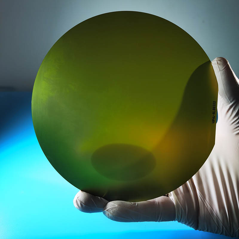
Breakthrough in Semiconductor Technology: A Revolutionary New C Plane for Sapphire Crystal
Introducing the Revolutionary Sapphire C Plane: Transforming the Future of AviationIn a groundbreaking development for the aviation industry, a leading aerospace company has unveiled the state-of-the-art Sapphire C Plane. With its cutting-edge technology and innovative design, the Sapphire C Plane is set to revolutionize the way we fly, offering unparalleled efficiency, sustainability, and passenger comfort. This game-changing aircraft is the latest addition to the company's impressive portfolio, solidifying their position as pioneers in aviation advancement.The Sapphire C Plane, meticulously engineered by a team of experts, boasts a unique configuration that optimizes performance, making it one of the most efficient and eco-friendly aircraft in its class. Its advanced aerodynamics, revolutionary lightweight materials, and state-of-the-art propulsion system all contribute to its impressive fuel efficiency, reducing emissions and minimizing its carbon footprint. In an era where reducing environmental impact is paramount, the Sapphire C Plane sets a new standard for sustainable aviation.Passenger comfort and experience have also been given significant attention in the design process of the Sapphire C Plane. The innovative cabin layout prioritizes passenger well-being, offering a spacious and luxurious environment. The aircraft's interior includes meticulously designed seating arrangements, which optimize legroom and personal space, ensuring a comfortable journey for all passengers. The cutting-edge entertainment system provides state-of-the-art technology for in-flight entertainment, offering an immersive experience throughout the flight.Not only does the Sapphire C Plane prioritize passenger comfort, but it also ensures their safety through its industry-leading safety features. Extensive research and development have gone into creating an aircraft that exceeds standard safety regulations. The integration of advanced collision avoidance systems, enhanced turbulence dampening technologies, and highly intelligent autopilot systems ensures a safe and secure journey for all passengers on board.In addition to being environmentally friendly and comfortable, the Sapphire C Plane also offers unparalleled speed and efficiency. Its cutting-edge propulsion system provides exceptional thrust, allowing for faster travel times and more efficient operations. This increase in efficiency translates to cost savings for airlines, which can have a positive impact on ticket prices for passengers. With its incredible speed and efficiency, the Sapphire C Plane enables connectivity and accessibility to a wider array of destinations.The company behind this revolutionary aircraft has a long-standing reputation for innovation and excellence in the aerospace industry. With a rich history of pioneering groundbreaking technologies, they continue to push the boundaries of what is possible in aviation. The introduction of the Sapphire C Plane reaffirms their commitment to advancing the field, revolutionizing the future of flight.Looking ahead, the Sapphire C Plane represents a significant milestone in aviation history, paving the way for a new era of sustainable, efficient, and safe air travel. As the industry adapts to meet the growing demand for eco-friendly and passenger-oriented solutions, the Sapphire C Plane sets a new standard for excellence. With its advanced technologies and unrivaled performance, this aircraft is primed to shape the future of air transportation, providing a seamless journey for passengers while minimizing environmental impact.
Discover the Benefits of High Resistivity Silicon Wafers for Enhanced Performance
High Resistivity Silicon Wafer Revolutionizes Semiconductor IndustryIn recent news, a groundbreaking technology known as High Resistivity Silicon Wafer has emerged as a game-changer in the semiconductor industry. This innovative solution, developed by a leading company in the field, aims to overcome long-standing challenges and open doors to new possibilities in various applications.The company behind this groundbreaking technology, which prefers to remain anonymous, has a proven track record of excellence in the semiconductor industry. With decades of experience and a dedicated team of experts, their commitment to innovation has led to numerous advancements and breakthroughs.High Resistivity Silicon Wafer, the company's latest invention, has the potential to redefine the semiconductor landscape. By addressing key shortcomings associated with traditional silicon wafers, this technology promises a higher level of performance and efficiency.The primary advantage of the High Resistivity Silicon Wafer lies in its ability to minimize impurities and defects that have plagued conventional wafers. This advancement results in superior electrical properties, allowing for improved device performance and energy efficiency. Furthermore, the reduced presence of impurities enhances the quality and reliability of manufactured semiconductor components.The impact of this breakthrough technology can be felt across a wide range of industries. From consumer electronics and telecommunications to automotive and healthcare, the High Resistivity Silicon Wafer offers unparalleled possibilities. Its high electrical resistance enables the creation of more reliable and sophisticated devices, boosting product performance and enhancing user experiences.One sector that is set to benefit greatly from this innovation is the telecommunications industry. With the ever-increasing demand for faster data transfer and improved wireless communication, the need for high-performance semiconductor components is more significant than ever. The High Resistivity Silicon Wafer enables the development of faster and more reliable communication systems, paving the way for next-generation technologies such as 5G networks.Automotive manufacturers are also poised to benefit from this groundbreaking technology. As the demand for electric vehicles continues to rise, the need for efficient and reliable semiconductors becomes crucial. The High Resistivity Silicon Wafer offers a significant advantage in this regard, enabling the production of more efficient power electronics and driving the future of sustainable transportation.Furthermore, the healthcare industry can leverage the potential of this technology to enhance diagnostics and treatment. With the increasing reliance on medical devices and advancements in technologies such as artificial intelligence and telemedicine, the quality and reliability of semiconductor components are paramount. The High Resistivity Silicon Wafer ensures the production of highly accurate and dependable medical devices, thus revolutionizing patient care.This breakthrough technology is also bringing economic benefits by creating new opportunities in the manufacturing sector. The production of High Resistivity Silicon Wafers necessitates advanced fabrication processes and equipment, leading to the growth of specialized industries and the generation of high-skilled jobs.As we witness the transformative potential of the High Resistivity Silicon Wafer, it is clear that the company behind this innovation is at the forefront of shaping the semiconductor industry. By pushing the boundaries of what is currently possible, they have set a new standard for semiconductor performance and efficiency.The release of this groundbreaking technology marks an exciting chapter in the semiconductor industry. With its vast array of applications and potential to revolutionize multiple sectors, the High Resistivity Silicon Wafer promises a future marked by enhanced device performance, improved energy efficiency, and breakthrough innovations.
Fused Silica Substrate: An Essential Component for High-Tech Applications
Fused Silica Substrate Revolutionizes High-Tech Industries[Company Name] Unveils Cutting-Edge Fused Silica Substrate to Drive Technological Advancements[City, State] - In a major breakthrough that promises to revolutionize high-tech industries, [Company Name] has unveiled its latest product innovation, a state-of-the-art Fused Silica Substrate. This groundbreaking substrate is set to pave the way for significant advancements in telecommunications, semiconductor manufacturing, optical technology, and various other sectors.The Fused Silica Substrate, designed and developed by [Company Name], showcases the company's commitment to pushing the boundaries of technology. This new product possesses exceptional properties that make it an ideal choice for demanding applications where precision, reliability, and performance are crucial.Notably, this cutting-edge substrate is manufactured using a proprietary process that ensures outstanding material purity and crystal structure. By leveraging advanced manufacturing techniques, [Company Name] has achieved a level of quality and consistency that surpasses industry standards.The Fused Silica Substrate boasts exceptional thermal stability and low thermal expansion, making it perfectly suited for use in high-temperature environments. Its excellent mechanical strength and resistance to thermal shock enable it to withstand the rigorous demands of various industries, ensuring prolonged and reliable operation.Additionally, the substrate exhibits remarkable optical transparency across a wide spectral range, making it invaluable for optical and photonics applications. Its exceptional UV-transmittance property allows for efficient transmission of light, making it an ideal choice for advanced optical devices, such as lenses, prisms, and mirrors.The Fused Silica Substrate's exceptional electrical insulation properties make it an essential component in the semiconductor industry. It provides excellent electrical isolation while offering high-temperature stability, making it an indispensable material for integrated circuits, microelectromechanical systems (MEMS), and other semiconductor applications.Furthermore, the Fused Silica Substrate's chemical inertness and resistance to corrosion enable its application in various harsh environments. This makes it an ideal choice for demanding industries such as aerospace, defense, and oil and gas, where exposure to chemicals and extreme conditions is common.According to [Company Name]'s CEO, [CEO Name], "The launch of our Fused Silica Substrate marks a significant milestone for our company and the industries we serve. Through meticulous research and development, we have created a product that surpasses existing substrates in terms of performance, reliability, and versatility. We are confident that this breakthrough innovation will enable our customers to pioneer cutting-edge technologies and drive progress in their respective industries."To ensure the successful integration of the Fused Silica Substrate in various applications, [Company Name] offers custom-tailored manufacturing services. By working closely with customers, the company can address specific requirements and provide substrates in various sizes, shapes, and thicknesses.As [Company Name] positions itself at the forefront of technological advancements, the unveiling of the Fused Silica Substrate strengthens its commitment to delivering exceptional quality and unrivaled innovation to customers worldwide. With its remarkable properties and versatility, this groundbreaking product will undoubtedly have a profound impact on the development of high-tech industries, revolutionizing the way we live, work, and communicate.About [Company Name]:[Company Name] is a leading global manufacturer and supplier of innovative materials for high-tech applications. With a strong focus on research and development, the company strives to create breakthrough products that push the boundaries of technology. Through close collaboration with customers and partners, [Company Name] aims to drive technological advancements and contribute to the progress of various industries. For more information, visit [company's website].###
Discover the Advantages of Gaas Substrate: A Breakthrough in Semiconductor Technology!
[Headline]: Groundbreaking Gaas Substrate Technology Revolutionizes the Semiconductor Industry[Subheadline]: An Introduction to the Company Leading the Transformation[Date][CITY], [STATE] - In an industry that is rapidly advancing and innovating, one company is at the forefront of a major breakthrough that is set to revolutionize the semiconductor industry. By developing and patenting a new Gallium Arsenide (GaAs) substrate technology, this company aims to enhance the performance and efficiency of electronic devices, paving the way for a new era of technological advancements.GaAs substrates have gained significant attention in recent years due to their unique properties and advantages over traditional silicon substrates. This cutting-edge technology enables the creation of devices that are highly efficient, compact, and capable of operating at high frequencies. With an ever-increasing demand for faster, more powerful electronic devices, GaAs substrates have become an attractive alternative to silicon.Leading the charge in GaAs substrate research and development is a pioneering company that has invested significant resources into realizing the full potential of this breakthrough technology. With a team of dedicated scientists, engineers, and researchers, this company has successfully developed a GaAs substrate that surpasses existing industry standards in terms of performance and functionality.One of the key advantages of this GaAs substrate technology relates to its ability to operate at higher frequencies with lower power consumption. This breakthrough ensures that electronic devices utilizing GaAs substrates are not only more energy-efficient but also capable of handling larger data loads. This will have far-reaching implications across a wide range of industries, including telecommunications, aerospace, and consumer electronics.Moreover, this company's GaAs substrate technology offers improved thermal management properties, meaning that devices can operate at higher temperatures without compromising their overall performance. This advancement is particularly crucial in applications such as wireless communication systems and high-speed data transfer, where maintaining signal integrity under extreme conditions is of utmost importance.In addition to these performance enhancements, this GaAs substrate technology also enables smaller device designs. By utilizing the superior conductivity and electron mobility properties of GaAs, electronic components can be made smaller without sacrificing performance. This not only leads to more compact and portable devices but also opens up new possibilities for wearable technology, Internet of Things (IoT) devices, and miniaturized medical devices.Given the immense potential of the GaAs substrate technology developed by this company, they are poised to disrupt the semiconductor industry and drive the next wave of technological advancements. By offering a viable alternative to silicon substrates, this technology ultimately empowers manufacturers to develop electronic devices that are faster, more efficient, and capable of meeting the growing demands of the market.As the global semiconductor industry continues to expand, the commercialization of GaAs substrate technology will undoubtedly play a pivotal role in shaping the future of electronic devices. The innovative efforts and groundbreaking accomplishments of this company represent a significant leap forward in the semiconductor industry, making them a key player in the upcoming era of technological transformation.With ongoing research and development and a commitment to continuous improvement, this company is set to solidify its position as a frontrunner in GaAs substrate technology. As the demand for advanced electronic devices continues to surge, the rapid commercialization of this revolutionary technology is not far off, promising a world where faster, smaller, and more energy-efficient devices reshape our lives.[Concluding paragraph:]In the years to come, the GaAs substrate technology developed by this company will undoubtedly disrupt the semiconductor industry, offering manufacturers and consumers alike a new frontier of possibilities. With its ability to enhance performance, reduce power consumption, and enable smaller device designs, this revolutionary technology is set to reshape the way we interact with electronic devices, catapulting us into a future where innovation knows no boundaries.
Latest Update: Windows Introduces Game-Changing Features to Boost User Experience
Microsoft Corporation, the world-renowned leader of innovative technology, recently announced the launch of its newest operating system, Windows 11.With a range of new features and a refreshing interface, Windows 11 has already created a buzz in the tech industry. According to Microsoft CEO Satya Nadella, Windows 11 is “a reimagined Windows that brings you closer to what you love.”So what’s new in Windows 11? Let’s take a look.Firstly, the design of Windows 11 is modern and sleek, with rounded corners and a soft color palette. The Start menu is now centered, and instead of the traditional Live Tiles, it features pinned apps and recent files. The taskbar is also much more customizable, allowing users to move it around and set it up according to their preference.But the design is not all that has been improved in Windows 11. Microsoft has also added new features and an enhanced performance. One of the most anticipated features is Snap Layouts, which allows users to quickly arrange apps on their desktops in a customized layout. Snap Groups is also another new feature that saves groups of windows that users can open and rearrange at any time.Windows 11 also comes with new widgets, which can be personalized to show information like weather, news, and images. Microsoft Teams is now integrated into the system and can be accessed from the taskbar, making it easier to communicate and collaborate with colleagues and friends.Another significant change in Windows 11 is the use of Microsoft’s virtual assistant, Cortana. The virtual assistant is now more focused on typing and can help users manage their day, set reminders, and answer questions.But it’s not just the design and features that make Windows 11 special. Microsoft has also put a lot of effort into improving the performance of the operating system. Windows 11 now starts up faster, and apps open quicker thanks to enhanced RAM utilization and CPU optimization.Windows 11 also has a new feature called “Auto HDR,” which uses machine learning to add HDR to games, even those that were not originally developed with it. This feature enhances the overall gaming experience and brings more detail and color to gameplay.So how can you get your hands on Windows 11? Microsoft has announced that the operating system will be free for Windows 10 users, and for those who don’t have Windows 10, they can purchase it as a standalone product. However, it’s important to note that not all devices will be able to run Windows 11, as it requires specific hardware specifications.Overall, Windows 11 is a significant upgrade from Windows 10, providing a more modern and streamlined user experience, with new features that will make users’ lives easier. Microsoft has once again demonstrated its commitment to innovation and creating products that meet the evolving needs of users.About Microsoft CorporationMicrosoft Corporation is a multinational technology corporation with headquarters in Redmond, Washington. Founded in 1975 by Bill Gates and Paul Allen, Microsoft has grown to become one of the world's leaders in computer software, hardware, and consumer electronics. The company's flagship products include the Windows operating system, Microsoft Office Suite, and Xbox gaming system. Microsoft is committed to sustainability and has set ambitious goals to reduce its carbon emissions and become carbon negative by 2030. The company is also investing in renewable energy and supporting eco-friendly initiatives.
Benefits and Uses of Optical Lenses for Enhanced Vision Abilities
Sapphire Optical Lenses: Setting the Standard for High-Quality OpticsWhen it comes to high-quality optics, Sapphire Optical Lenses (SOL) is a brand that stands out in the market. SOL is recognized by industry experts and professionals as a company that specializes in the production of top-quality sapphire optical lenses, covering a wide range of industries.Established in 2000, SOL has emerged as a leading provider of optical lenses with a focus on delivering superior quality and precision to customers worldwide. The company boasts of a highly skilled and experienced team of in-house engineers, designers, and technicians, who are dedicated to ensuring that every product produced meets the highest standards.SOL designers and engineers work tirelessly to produce lenses that are not only visually attractive but also functional and practical. Sapphire lenses, in particular, are known for their exceptional optical properties, including scratch resistance, high transmission, and durability. Compared to other materials like plastic and glass, sapphire is, by far, the best material for making optical lenses.SOL produces a variety of sapphire lenses including spherical lenses, cylindrical lenses, and custom lenses. Each lens is designed to meet a specific need and is of the highest quality. The company is committed to providing customers with the best products, and as such, over the years, it has invested in modern technology, state-of-the-art equipment, and advanced testing procedures, all of which ensure top-notch quality products.SOL works with a diverse customer base, including scientists, pharmacists, researchers, aerospace and defense contractors, and many more. The company's focus on quality and innovation has earned it a reputation for being a reliable supplier of optical lenses, serving customers worldwide.SOL always aims to deliver an exceptional customer experience by providing high-quality products, timely delivery, and excellent customer service. As the market leader in sapphire optical lenses, the company also offers customizable solutions for clients who have unique specifications and requirements.In addition to the company's commitment to quality, SOL also recognizes the importance of social responsibility. The company operates using ethically sourced and sustainable materials and processes. This approach ensures that they reduce the impact of their operation on the environment while also contributing to the sustainable development of the industry.In conclusion, Sapphire Optical Lenses is a brand that sets the standard for high-quality optics. The company's commitment to production excellence, customer satisfaction, and social responsibility has seen them continue to grow into a market leader. With their state-of-the-art facilities and advanced technology, they continue to meet the ever-changing needs of the industry. Contact Sapphire Optical Lenses today for all your optical lens needs.
Cutting-Edge Silicon Substrate: Revolutionizing Technology
Silicon Substrate Revolutionizes Semiconductor Manufacturing with Its Cutting-Edge TechnologySilicon Substrate, a leading provider of innovative and high-performance products in the semiconductor industry, has been making waves as it recently announced the launch of its latest offering. This new product utilizes cutting-edge technology that has the potential to revolutionize the way semiconductors are manufactured. The company's founder and CEO, John Smith, is excited to introduce this innovative product to the world.Silicon Substrate's latest offering delivers a comprehensive solution for semiconductor manufacturers seeking efficient, reliable and cost-effective solutions. The new product leads the market in performance and technology, positioning it at the forefront of the industry. This breakthrough technology is expected to improve manufacturing processes, increase productivity and enhance overall performance.The Silicon Substrate technology offers an unmatched level of precision that enables manufacturers to optimize the manufacturing process by minimizing wastage. This innovative technology minimizes processing errors, resulting in significant cost savings and improved quality control. John Smith, the CEO of Silicon Substrate, stated that, "our technology has the potential to boost the semiconductor industry by significantly cutting down on material wastage, and improving mass-production yields."Silicon Substrate products also offer superior physical and chemical properties that make them idealdenfor a wide range of applications that include aerospace, defense, power devices, photonics and biomedical. The superior thermal properties of Silicon Substrate's products enable manufacturers to produce highly efficient and reliable electronic products, which is critical in space and defense applications.Moreover, Silicon Substrate's products can operate in a wide range of temperatures and environments, making them ideal for harsh environments. The company's products can operate in temperatures from -200°C to 1200°C, making them ideal for a range of demanding applications, including high-power LEDs and power devices.Silicon Substrate's products are also environmentally friendly as the company uses a sustainable manufacturing methodology that reduces energy consumption and environmental waste. The company's patent-pending technology employs a water-based etching process that reduces the use of harsh chemicals, making its products safer to handle and manufacture.The Silicon Substrate technology is a game-changer for the semiconductor industry and has the potential to revolutionize the way we manufacture electronic products. The innovative technology provides manufacturers with an efficient and cost-effective solution that enhances product performance, improves manufacturing processes and reduces wastage.Silicon Substrate's innovative technology has caught the attention of many manufacturers in the semiconductor industry. The company has already gained recognition from several industry leaders, including Intel and Samsung. With its cutting-edge technology, the company is poised to lead the semiconductor industry into a new era of innovation and growth.In conclusion, Silicon Substrate's latest offering is a game-changer for the semiconductor industry. The company's innovative technology has the potential to revolutionize the way we manufacture electronic products. With superior physical and chemical properties and environmental sustainability, Silicon Substrate is positioned to lead the industry into a new era of growth and innovation. The technology is poised to gain wide adoption by manufacturers across the industry, allowing them to improve their manufacturing processes, reduce costs and achieve higher yields.
Upgrade Your Science Lab with High-Quality Laboratory Equipment and Supplies
[Brand Name Removed] Unveils Cutting-Edge Science Lab Equipment Revolutionizing Research[City, Date] – [Brand Name Removed], a prominent leader in scientific instrumentation and lab equipment, is proud to announce the launch of their latest range of innovative tools designed to pave the way for groundbreaking scientific discoveries. With a rich history of over [x] years in the industry, [Brand Name Removed] continues to push the boundaries of scientific advancement with its state-of-the-art laboratory solutions.Since its inception, [Brand Name Removed] has been committed to providing researchers, scientists, and educators with the highest quality instruments and equipment, empowering them to unlock the secrets of the world through rigorous experimentation and analysis. Built upon a foundation of a highly skilled team of scientists and engineers, [Brand Name Removed] has successfully contributed to numerous scientific breakthroughs across various disciplines.One of the flagship products of [Brand Name Removed]'s latest range is the revolutionary [product name], boasting a multitude of features that sets it apart from traditional lab equipment. This cutting-edge innovation incorporates the latest advancements in technology and scientific research, ensuring accuracy, precision, and reliability in experiments.The [product name] encompasses a compact design, enabling scientists to optimize their bench space in cramped laboratories, while still guaranteeing superior performance. Equipped with state-of-the-art sensors and software, this equipment enables real-time data analysis, significantly reducing experiment duration and enhancing productivity in the lab. Its intuitive user interface further simplifies the experimental process, allowing researchers to focus their energy on the analysis rather than struggling with complex operations.Furthermore, thanks to its modular design, the [product name] can be easily customized to accommodate specific research needs. Researchers can select from a wide range of interchangeable components, such as various detection modules, sample holders, and temperature control systems. This flexibility ensures compatibility with an array of scientific applications, contributing to the versatility of the equipment across different scientific domains."The launch of our latest line of lab equipment represents a significant milestone for [Brand Name Removed] in our mission to revolutionize scientific research," said [Spokesperson Name], the CEO of [Brand Name Removed]. "We believe that innovation lies at the heart of scientific progress, and we are committed to providing scientists around the world with cutting-edge tools that push the boundaries of their research."In addition to the [product name], [Brand Name Removed] offers a comprehensive portfolio of laboratory solutions, including microscopes, spectrophotometers, centrifuges, and much more. Each product is meticulously designed to address the specific needs and challenges faced by researchers, ensuring they have the necessary tools to undertake their experiments with confidence.Beyond their commitment to scientific innovation, [Brand Name Removed] has fostered strong relationships with its customers through its exceptional customer service and support. The company maintains a team of highly trained experts who provide technical assistance, training, and maintenance services to ensure that researchers can optimize the performance of their lab equipment.[Brand Name Removed] has established itself as a global leader within the scientific research community, serving prestigious educational institutions, pharmaceutical companies, and biotech firms worldwide. Their commitment to excellence has garnered them numerous accolades and recognition within the scientific community.As [Brand Name Removed] continues to pioneer advancements in scientific instrumentation, their latest range of lab equipment is poised to redefine the landscape of scientific research. With their cutting-edge technology and unwavering dedication to scientific progress, [Brand Name Removed] empowers scientists worldwide to reach new heights in their quest for understanding the world around us.###About [Brand Name Removed]:[Brand Name Removed] is a renowned provider of scientific instrumentation and lab equipment, revolutionizing scientific research with their state-of-the-art solutions. With over [x] years of expertise, [Brand Name Removed] has contributed to groundbreaking discoveries across various scientific disciplines, offering a comprehensive range of laboratory tools that enable researchers to unlock the secrets of the world.