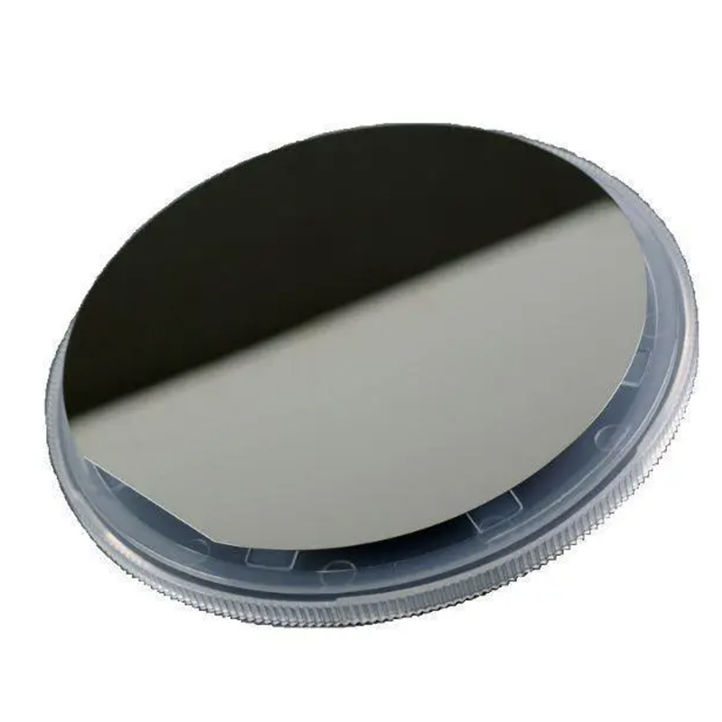
High-Quality Silicon Oxide Wafer: Everything You Need to Know

By:Admin on 2025-02-27 02:27:16

Silicon Oxide Wafer, a new product offered by a leading semiconductor company, is set to revolutionize the semiconductor industry with its cutting-edge technology. This innovative product is expected to have a significant impact on various sectors, including electronics, automotive, and healthcare.The Silicon Oxide Wafer is a crucial component in the manufacturing of semiconductor devices. It is a highly advanced material that offers superior performance and reliability compared to traditional wafers. The product is designed to meet the growing demand for high-quality semiconductor devices that can operate efficiently in a wide range of applications.The company behind this groundbreaking product has a solid reputation in the semiconductor industry. With several decades of experience in producing high-performance components, they have established themselves as a trusted supplier for many leading companies in the electronics and semiconductor sectors.The Silicon Oxide Wafer is the latest addition to the company's extensive portfolio of semiconductor products. It is the result of years of research and development, aimed at creating a material that can meet the evolving needs of the semiconductor industry. The company has invested heavily in state-of-the-art manufacturing facilities and cutting-edge technologies to ensure the highest quality standards for its products.One of the key advantages of the Silicon Oxide Wafer is its superior thermal and electrical properties. This enables semiconductor devices to operate at higher temperatures and with lower power consumption, making them ideal for a wide range of applications. Additionally, the wafer offers exceptional mechanical strength and reliability, ensuring that the semiconductor devices built on it can withstand harsh operating conditions.The company has also invested in developing environmentally friendly manufacturing processes for the Silicon Oxide Wafer. By using sustainable materials and energy-efficient production methods, they are committed to reducing their environmental impact and contributing to a more sustainable future for the semiconductor industry.The launch of the Silicon Oxide Wafer has generated significant interest within the semiconductor industry. Many leading companies have already expressed their intention to incorporate this innovative material into their semiconductor devices. This is expected to drive rapid adoption of the product across various applications, further solidifying the company's position as a key player in the semiconductor market.In addition to its technical capabilities, the Silicon Oxide Wafer is also expected to offer cost savings for semiconductor manufacturers. Its advanced properties can lead to higher yields and improved manufacturing efficiency, resulting in lower production costs and increased profitability for semiconductor companies.With the introduction of the Silicon Oxide Wafer, the company aims to strengthen its position as a leading provider of high-performance semiconductor materials. They are confident that this breakthrough product will help shape the future of the semiconductor industry and drive innovation in electronic devices, automotive systems, and healthcare technologies.The company is committed to continuing its investment in research and development to further advance the capabilities of the Silicon Oxide Wafer and other semiconductor products. By staying at the forefront of technological advancements, they aim to address the growing demands of the semiconductor industry and support the development of next-generation electronic devices.Overall, the launch of the Silicon Oxide Wafer represents a significant milestone for the semiconductor industry. With its advanced properties and potential for widespread adoption, this product is expected to have a transformative impact on various sectors, paving the way for the development of highly efficient and reliable semiconductor devices. The company's dedication to innovation and sustainability positions them as a key player in driving the future of the semiconductor industry.

Read More

Understanding Wafer Crystal Orientation: A Complete Guide

By:Admin on 2025-02-24 03:21:11

Established in [year], {Company} has been a leader in the manufacturing and distribution of cutting-edge wafer technology. Specializing in wafer crystal orientation, {Company} has cemented its position as a global innovator in the semiconductor industry. With a commitment to providing high-quality products and exceptional customer service, {Company} has continued to push the boundaries of wafer technology, meeting the demands of an ever-evolving market.Wafer crystal orientation is a critical process in the semiconductor industry, determining the physical and electrical properties of the wafer. By precisely controlling the crystal orientation, manufacturers can optimize the performance of the semiconductor devices, leading to improved efficiency and functionality. {Company} has been at the forefront of developing advanced techniques for wafer crystal orientation, offering a range of orientation options to meet specific customer requirements.One of the key factors that set {Company} apart is its dedication to research and development. The company's team of experts continuously works to refine and enhance the wafer crystal orientation process, incorporating the latest advancements in material science and crystallography. This relentless pursuit of innovation has allowed {Company} to stay ahead of the curve, delivering cutting-edge solutions that exceed industry standards.In addition to its commitment to technological advancement, {Company} places a strong emphasis on quality control. The company's state-of-the-art manufacturing facilities adhere to rigorous quality standards, ensuring that every wafer meets the highest level of precision and performance. By maintaining strict quality control measures, {Company} has earned a reputation for reliability and consistency, attracting a loyal customer base from around the world.As part of its comprehensive range of products and services, {Company} offers custom wafer crystal orientation options, allowing customers to tailor the orientation specifications to their exact needs. This flexibility enables semiconductor manufacturers to achieve optimal results in their specific applications, whether it's for consumer electronics, automotive systems, or industrial machinery. With a focus on customization and personalized support, {Company} is committed to helping its customers achieve their unique objectives.The impact of {Company}'s wafer crystal orientation technology extends far beyond the semiconductor industry. Its products play a critical role in a wide range of applications, from advanced computing and telecommunications to renewable energy and medical devices. This broad reach underscores the importance of wafer technology in shaping the future of technology and innovation.Looking ahead, {Company} remains dedicated to pushing the boundaries of wafer crystal orientation, as it continues to explore new avenues for improvement and expansion. With a relentless focus on innovation, quality, and customer satisfaction, {Company} is poised to lead the way in the semiconductor industry for years to come.In conclusion, {Company} has established itself as a leader in wafer crystal orientation, delivering cutting-edge solutions that drive the semiconductor industry forward. Through its commitment to research and development, quality control, and customer-centric approach, {Company} has earned a reputation for excellence and innovation. As the demand for advanced semiconductor technology continues to grow, {Company} is well-positioned to meet the evolving needs of the industry, shaping the future of technology with its groundbreaking wafer products and services.

Read More

Single Crystal Al2O3: Properties, Production, and Applications

By:Admin on 2025-02-20 02:27:28

Al2O3 Single Crystal: Revolutionizing the Semiconductor IndustryWith the rapid advancement of technology, the demand for high-performance semiconductor materials has been on the rise. To meet this increasing demand, {company name}, a leading manufacturer of advanced materials, has developed Al2O3 single crystal, a breakthrough material that is set to revolutionize the semiconductor industry.Al2O3 single crystal, also known as sapphire (Al2O3), is a remarkable material with a wide range of applications. Its unique combination of properties, including high transparency, high thermal conductivity, excellent mechanical strength, and chemical resistance, makes it an ideal material for various semiconductor and optoelectronic applications.As a pioneer in the development of advanced materials, {company name} has been at the forefront of producing high-quality Al2O3 single crystal. Through years of research and development, the company has perfected the growth process of Al2O3 single crystal, ensuring the material's exceptional purity and structural integrity. This has enabled {company name} to establish itself as a trusted supplier of Al2O3 single crystal to leading semiconductor manufacturers around the world.One of the key advantages of Al2O3 single crystal is its high thermal conductivity, which allows for efficient heat dissipation in electronic devices. This makes it an ideal material for use in high-power semiconductor devices such as radio frequency (RF) transistors and power electronics. Additionally, its excellent optical properties, including high transmission in the UV to IR range, make it well-suited for use in optical windows and lenses for laser and imaging applications.Furthermore, Al2O3 single crystal exhibits exceptional mechanical strength and chemical resistance, making it an ideal material for use in harsh operating environments. Its durability and resistance to chemical corrosion make it suitable for use in semiconductor processing equipment, where it can withstand the high temperatures and harsh chemical conditions encountered during semiconductor fabrication processes.In addition to its physical properties, Al2O3 single crystal is also an environmentally friendly material. It is non-toxic and non-reactive, making it a sustainable choice for semiconductor and optoelectronic applications. As the industry continues to prioritize sustainability and environmental responsibility, the use of Al2O3 single crystal can help semiconductor manufacturers reduce their environmental impact.With the increasing demand for high-performance semiconductor materials, the development of Al2O3 single crystal is poised to have a significant impact on the industry. Its unique combination of properties makes it an attractive material for a wide range of applications, from high-power electronics to optical components. As a result, {company name} is well-positioned to play a key role in meeting the growing demand for Al2O3 single crystal from semiconductor manufacturers around the world.In conclusion, the development of Al2O3 single crystal by {company name} represents a significant advancement in the semiconductor industry. With its exceptional properties and wide range of applications, this breakthrough material is set to revolutionize the way semiconductor devices are designed and manufactured. As the industry continues to evolve, Al2O3 single crystal will undoubtedly play a pivotal role in enabling the development of next-generation electronic and optoelectronic devices.

Read More