
New Technology Breakthrough: High-Quality Sapphire Ingot Unveiled
By:Admin
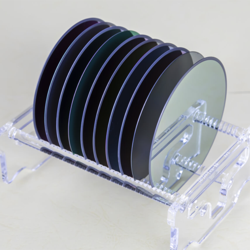
Founded in [], {} has quickly established itself as a leader in the sapphire industry. The company's state-of-the-art production facilities and expertise in crystal growth technology have enabled it to produce sapphire ingots of the highest quality. By employing advanced techniques such as the Kyropoulos method, {} has been able to fabricate sapphire ingots that meet the stringent requirements of its diverse customer base.
One of the key strengths of {} lies in its vertically integrated production process. From the selection of raw materials to the final inspection of sapphire ingots, the company maintains strict quality control standards at every stage of manufacturing. This comprehensive approach has allowed {} to consistently deliver sapphire ingots that exceed industry benchmarks in terms of purity, crystal structure, and overall performance.
In addition to its cutting-edge manufacturing capabilities, {} also prides itself on its research and development activities. The company's team of materials scientists and engineers are constantly pushing the boundaries of sapphire ingot technology, seeking to develop new formulations and manufacturing processes that will further enhance the properties of sapphire ingots. By staying at the forefront of technological advancements, {} continues to solidify its position as a leading supplier of sapphire ingots in the global market.
The demand for sapphire ingots has been steadily increasing in recent years, driven by the growing adoption of sapphire-based devices and components in various industries. As a result, {} has been ramping up its production capacity to meet the needs of its expanding customer base. The company's commitment to scalability and efficiency has allowed it to respond quickly to market demands, ensuring that it can supply sapphire ingots in large quantities without compromising on quality.
Furthermore, {} has been actively expanding its presence in international markets, forging strategic partnerships with key players in the sapphire industry. By leveraging its extensive network of distributors and collaborators, {} has been able to reach customers in different regions and cater to their specific requirements. This global approach has not only opened up new business opportunities for {} but has also contributed to the widespread adoption of sapphire ingots across diverse applications.
Looking ahead, {} is poised to maintain its leadership in the sapphire ingot market through continued investment in research and development, as well as the expansion of its production capabilities. By staying ahead of technological advancements and market trends, {} is well-equipped to meet the evolving needs of its customers and contribute to the ongoing innovation in the sapphire industry.
In conclusion, the growing demand for sapphire ingots is driving significant advancements in the materials science and technology sectors. With its expertise in sapphire ingot manufacturing and its commitment to excellence, {} is poised to play a key role in shaping the future of sapphire-based products and applications. As the company continues to push the boundaries of what is possible with sapphire ingots, it is likely to remain a dominant force in the global market for years to come.
Company News & Blog
Silicon Carbide Ceramic: Unleashing the Power of Advanced Ceramic Materials
Title: Enhancing Efficiency and Durability: The Cutting-Edge Silicon Carbide Ceramic from {Company}Subtitle: Innovations in Material Science Propel Advancements in Various Industries[City, Date] - {Company}, a leading provider of advanced engineering solutions, is set to revolutionize various industries with their groundbreaking Silicon Carbide Ceramic technology. Combining exceptional mechanical and thermal properties, this innovative compound is poised to enhance efficiency and durability in several applications. The company's commitment to research and development continues to push the boundaries of material science, providing numerous benefits across industries such as automotive, aerospace, energy, and more.{Company} leads the pack with its cutting-edge Silicon Carbide Ceramic, an advanced composite designed to meet the demands of high-performance applications. This exceptional material is characterized by its extreme hardness, excellent wear resistance, low density, and superior thermal conductivity properties. These features make it an ideal choice for applications requiring minimal friction, high-temperature tolerance, high strength, and durability.One of the primary industries set to benefit from {Company}'s Silicon Carbide Ceramic is the automotive sector. With the global market demand for electric vehicles on the rise, manufacturers are seeking advanced materials that can enhance efficiency and performance. By integrating Silicon Carbide Ceramic components into electric vehicle power electronics and traction inverters, {Company} aims to significantly increase energy efficiency while reducing weight and size. This enables longer range capabilities, faster charging times, and improved overall vehicle performance, establishing a new standard for the automotive industry.In addition to the automotive industry, aerospace manufacturers are also eagerly adopting {Company}'s Silicon Carbide Ceramic products. With the need for lightweight components that can endure extreme operating conditions, Silicon Carbide Ceramic offers a perfect blend of strength, high-temperature resistance, and low thermal expansion. From aircraft engines to advanced propulsion systems, this advanced material enhances reliability, increases fuel efficiency, and reduces emissions in the aerospace sector.Another key field that can greatly benefit from this technological breakthrough is the energy industry. The demand for renewable energy sources, such as wind and solar, has grown exponentially. {Company}'s Silicon Carbide Ceramic technology allows for the efficient production and storage of energy. Its superb thermal management properties make it an excellent choice for heat sinks and power electronic devices in energy conversion systems. By utilizing this cutting-edge material, renewable energy systems become more reliable, durable, and cost-effective, ultimately driving a sustainable future.Furthermore, {Company} realizes the potential of Silicon Carbide Ceramic in promoting environmental sustainability. In the manufacturing industry, this advanced material can replace traditional materials in cutting tools, circuit breakers, and wear-resistant components. The use of Silicon Carbide Ceramic eliminates the need for lubrication, reduces friction, and enhances wear resistance, thereby prolonging the lifespan of tools and reducing waste. Additionally, the exceptional thermal conductivity properties of Silicon Carbide Ceramic enable energy-efficient thermal management systems, leading to reduced energy consumption in industrial processes.{Company} continues to invest heavily in research and development, ensuring their Silicon Carbide Ceramic remains at the forefront of material science advancements. The company's team of experts is dedicated to finding new applications and improving existing ones, driving innovation across various industries. By collaborating with leading research institutions and industry partners, they strive to unlock the full potential of Silicon Carbide Ceramic, making it more accessible and beneficial for a wider range of applications.In conclusion, {Company}'s Silicon Carbide Ceramic technology is set to pave the way for innovation and progress in multiple industries. Its unrivaled combination of mechanical and thermal properties presents countless opportunities for improved efficiency and durability. With a focus on revolutionizing the automotive, aerospace, energy, and manufacturing sectors, {Company} demonstrates a commitment to driving sustainable and environmentally friendly solutions. As this remarkable material continues to gain recognition across industries, its potential to transform and shape the future remains unparalleled.
Ultimate Guide to 12 Inch Wafers: Everything You Need to Know
12 Inch Wafer Revolutionizes Semiconductor IndustryAs the demand for smaller, faster, and more powerful electronic devices continues to grow, the semiconductor industry is constantly striving to push the boundaries of technology. One company that is at the forefront of this revolution is [company name]. With its cutting-edge 12 inch wafer technology, [company name] is set to reshape the semiconductor landscape and unlock new possibilities for the next generation of electronic devices.Founded in [year], [company name] has always been dedicated to pushing the boundaries of innovation in the semiconductor industry. With a strong focus on research and development, the company has continuously invested in state-of-the-art manufacturing facilities and advanced technologies to stay ahead of the competition. This commitment to innovation has allowed [company name] to become a leading player in the global semiconductor market, with a reputation for delivering high-quality, high-performance products.The latest milestone in [company name]'s journey of innovation is the development of the 12 inch wafer technology. Traditionally, semiconductor wafers have been produced in smaller sizes, such as 8 inch or 6 inch, limiting the number of chips that can be produced on each wafer. However, with the introduction of the 12 inch wafer, [company name] has significantly increased the manufacturing capacity and efficiency, resulting in a dramatic improvement in output and cost-effectiveness.The 12 inch wafer technology is a game-changer for the semiconductor industry, as it allows for the production of more chips per wafer, reducing manufacturing costs and ultimately offering more competitive pricing for consumers. This breakthrough also enables the development of more advanced and powerful electronic devices, as the larger wafers provide greater flexibility for designing and manufacturing complex semiconductor components.In addition to the technological advancements, [company name] has also made significant investments in building a sustainable and eco-friendly manufacturing process for the 12 inch wafers. The company has implemented state-of-the-art cleanroom facilities and advanced manufacturing techniques to minimize waste and reduce environmental impact. By embracing sustainable practices, [company name] is not only contributing to the advancement of technology but also setting new standards for environmentally responsible manufacturing in the semiconductor industry.The impact of [company name]'s 12 inch wafer technology is already being felt across the semiconductor industry. Major players in the consumer electronics, automotive, and telecommunications sectors have expressed great interest in adopting the 12 inch wafer technology to enhance their product offerings and meet the growing demand for more advanced electronic devices.Furthermore, the widespread adoption of the 12 inch wafer technology is expected to drive significant growth in the semiconductor market, creating new opportunities for [company name] and its partners. As the demand for high-performance semiconductor components continues to rise, [company name] is well-positioned to capitalize on this trend and further solidify its position as a leading provider of innovative semiconductor solutions.Looking ahead, [company name] remains committed to driving innovation and shaping the future of the semiconductor industry. With its groundbreaking 12 inch wafer technology and strong emphasis on sustainability, the company is poised to make a lasting impact on the electronic devices of tomorrow.In conclusion, the introduction of the 12 inch wafer technology by [company name] represents a significant milestone in the semiconductor industry. This breakthrough is set to revolutionize the way semiconductor components are manufactured, enabling the development of more advanced and powerful electronic devices. With its relentless commitment to innovation and sustainability, [company name] is leading the charge towards a brighter and more efficient future for the semiconductor industry.
Solar Silicon Wafer Market Gains Momentum: A Promising Outlook for Growing Photovoltaic Industry
SolarTech Inc., a leading innovator in the solar energy industry, has recently announced the launch of their revolutionary Solar Silicon Wafer, a groundbreaking technology that promises to enhance the efficiency and reliability of solar panels. With this cutting-edge innovation, SolarTech aims to make a significant contribution to the global transition towards renewable energy sources.Solar energy has gained immense popularity in recent years as the world increasingly seeks sustainable alternatives to traditional sources of power. However, the efficiency of solar panels has been a persistent challenge in fully realizing the potential of this renewable energy source. SolarTech recognized this obstacle and set out to develop a solution that would revolutionize the solar industry.The newly introduced Solar Silicon Wafer is a game-changer in the solar energy sector. By combining advanced materials and state-of-the-art technology, SolarTech has created a high-performance silicon wafer that boasts unparalleled efficiency and durability. This breakthrough innovation not only maximizes the conversion of sunlight into electricity but also ensures the longevity of solar panels, making them a more reliable and cost-effective solution.The key to the superior performance of SolarTech's Solar Silicon Wafer lies in its unique composition and manufacturing process. The company employs a proprietary technique that allows them to produce silicon wafers with enhanced crystal structures, resulting in higher conversion rates and improved overall efficiency. Furthermore, SolarTech utilizes a combination of anti-reflective coatings and passivation layers to minimize energy loss and increase the durability of the wafer.One of the standout features of SolarTech's Solar Silicon Wafer is its ability to capture a broader spectrum of light, including both visible and infrared wavelengths. Traditional solar panels often struggle to harness infrared light, leading to a significant loss of potential energy. By overcoming this limitation, SolarTech's wafer can generate more electricity from the same amount of sunlight, significantly increasing the overall efficiency of solar panels.Another advantage offered by SolarTech's Solar Silicon Wafer is its strength and resilience. The company employs innovative manufacturing techniques that result in a highly durable wafer, capable of withstanding extreme weather conditions and harsh environments. This durability ensures that solar panels utilizing SolarTech's wafer are longer-lasting, providing a more sustainable and cost-effective solution for consumers and businesses alike.SolarTech's commitment to sustainability extends beyond their groundbreaking product. The company is dedicated to minimizing its environmental impact throughout the manufacturing and distribution processes. SolarTech has implemented several initiatives to reduce waste generation, optimize energy consumption, and lower greenhouse gas emissions. By prioritizing sustainability, SolarTech aims to lead by example and inspire others in the solar industry to adopt eco-friendly practices.The introduction of SolarTech's Solar Silicon Wafer has garnered significant attention from industry experts and consumers alike. The groundbreaking technology holds the potential to drive the mass adoption of solar energy by addressing the efficiency and reliability concerns that have hindered its progress. As countries continue to make ambitious commitments towards reducing greenhouse gas emissions and combating climate change, SolarTech's advanced silicon wafer could play a pivotal role in harnessing the power of the sun on a global scale.In conclusion, SolarTech Inc. has unveiled their revolutionary Solar Silicon Wafer, a groundbreaking technology that promises to revolutionize the solar energy industry. With its unmatched efficiency, durability, and ability to capture a broader spectrum of light, SolarTech's wafer sets a new standard for solar panel performance. The company's commitment to sustainability further solidifies their position as a leading innovator in the renewable energy sector. As the world strives towards a greener future, SolarTech's Solar Silicon Wafer offers a promising solution that could propel the adoption of solar energy to unprecedented heights.
Revolutionary Single Lens Glasses to Provide Enhanced Vision Experience
[Company Name] Introduces Innovative Single Lens Glasses, Revolutionizing Vision Correction[City, Date] — [Company Name], a leading innovator in the eyewear industry, has recently unveiled its groundbreaking creation - Single Lens Glasses. By combining state-of-the-art technology with exceptional design, these glasses promise to revolutionize the way people correct their vision.Vision correction has always been a crucial aspect of daily life for millions of individuals around the world. Traditional eyewear often includes the use of multiple lenses, adding bulk and weight to the final product. Single Lens Glasses, on the other hand, eliminate the need for multiple lenses by incorporating advanced optics into a single lens.With this breakthrough technology, [Company Name] aims to provide a more streamlined and comfortable vision correction experience. The elimination of multiple lenses not only reduces the weight and thickness of the glasses but also enhances the visual clarity for wearers.To achieve this innovative design, [Company Name] utilized cutting-edge manufacturing techniques and the highest quality materials. The company's team of optical experts and engineers worked tirelessly to ensure that the Single Lens Glasses offer exceptional performance while maintaining a sleek and stylish appearance.The patented lens design of the Single Lens Glasses provides wearers with a wider field of view compared to traditional eyewear. This expanded visual range allows users to see objects with greater clarity, enhancing their overall experience in various everyday activities.One key feature that sets the Single Lens Glasses apart from other eyewear options is its versatility. These glasses can be customized to accommodate various vision correction needs, including nearsightedness, farsightedness, and astigmatism. Wearers can easily adjust the prescription strength of the lenses, ensuring a tailored and personalized solution for their individual requirements.Comfort is another aspect that [Company Name] focused on while developing the Single Lens Glasses. The glasses are designed to fit comfortably on different face shapes and sizes, ensuring a secure fit throughout the day. The single lens construction also minimizes distortion and reduces eye strain, providing wearers with unparalleled comfort even during extended periods of use.In addition to its practical advantages, Single Lens Glasses also offer a range of fashionable options to suit different style preferences. The frames are available in a wide array of designs, materials, and colors, allowing wearers to express their personalities while enjoying optimal vision correction."We are thrilled to introduce our latest innovative creation, Single Lens Glasses," said [Spokesperson Name], the CEO of [Company Name]. "At [Company Name], we are committed to pushing boundaries and delivering cutting-edge eyewear solutions to our customers. With Single Lens Glasses, we have revolutionized the vision correction landscape, offering a game-changing product that combines performance, style, and comfort."As the eyewear industry continues to evolve, [Company Name] remains at the forefront of innovation. With the introduction of Single Lens Glasses, the company reinforces its commitment to providing groundbreaking solutions that enhance the quality of life for individuals in need of vision correction.The Single Lens Glasses are expected to be available for purchase in select retail stores and online platforms starting from [Date]. For more information about [Company Name] and its product range, please visit [Website].[Contact Information]About [Company Name]:[Company Name] is a leading innovator in the eyewear industry, dedicated to providing cutting-edge solutions for vision correction. With a strong focus on technological advancements and exceptional design, the company has established itself as a trusted brand among consumers worldwide. [Company Name] continues to push boundaries, developing eyewear products that combine performance, style, and comfort to enhance the vision correction experience.
How to Choose and Install Quality MGO Wafer Windows
In a world where environmental concerns are taking precedence over tradition, there is no better time for a company to introduce products that prioritize sustainability and energy efficiency. That is where MGO wafer windows come in. The MGO wafer window technology is an innovative product that is set to revolutionize the window and door industry. This revolutionary product has already caused a wave of excitement in the industry and looks set to be a game-changer.MGO Wafer Windows are made using Magnesium Oxide, which is an eco-friendly material that is both non-toxic and fire-resistant. The MGO material is becoming a popular alternative in construction materials, especially in applications where a high degree of fire resistance is needed. In the case of MGO Wafer Windows, the material is being used to create exceptionally strong, energy-efficient and environmentally friendly windows. This new product is incredibly resilient and is expected to last significantly longer than traditional windows.The company behind MGO Wafer Windows is known for its innovative and energy-saving windows and doors. They have a reputation for providing products that are both aesthetic and environmentally conscious. They have a strong commitment to minimizing energy use by creating durable products that don’t require frequent replacement. This new product is no exception. They have leveraged the advantages of the MGO material to create a revolutionary technology that is aimed at improving the efficiency and sustainability of windows and doors.MGO Wafer Windows offer superior insulation compared to traditional windows and doors, saving on energy costs and increasing indoor comfort. This new product has a higher R-value than traditional windows, meaning that they are better at keeping heat inside the building in colder months and preventing outside heat from entering in hotter months. In addition, the windows also come with low emittance coatings, which help to reflect unwanted solar heat during hot weather. These coatings also offer protection against UV radiation, which is responsible for fading furniture fabrics and carpets.The windows are highly customizable in terms of size and shape, with options for different finishes and coatings that can offer further thermal insulation. Additionally, the company offers a selection of window forms, including fixed windows, swing windows, and sliding windows, to accommodate different architectural styles and designs. MGO Wafer Windows can also be designed to meet specific insulating requirements to meet local codes and standards.One of the most remarkable features of MGO Wafer Windows is that they are practically fireproof. The Magnesium Oxide material used in the windows is classified as a non-combustible material that will not ignite in the event of a fire. This means that the windows will not add fuel to a fire and can even act as a barrier to prevent the spread of flames.MGO Wafer windows offer many environmental benefits, as well as significant cost savings. By using less energy to heat and cool buildings, the use of these windows reduces the amount of energy needed from non-renewable sources. Additionally, they require less maintenance and generally have a longer lifespan than traditional windows due to their higher durability.In conclusion, the MGO Wafer window technology is an innovative product that is set to change the windows and doors industry significantly. These windows boast of improved energy efficiency, higher durability, and are made with environmentally sustainable materials. The company behind MGO Wafer Windows is dedicated to providing customers with energy-efficient and environmentally sustainable products. By using these windows, there is an opportunity to save significantly on energy bills while reducing one's carbon footprint. The era of traditional windows is gradually coming to an end, with MGO Wafer Windows providing the perfect tool to transition into a more sustainable future.
Discover the Latest Advances in Silicon Wafer Chip Technology
Silicon Wafer Chips, a cutting-edge technology company based in Silicon Valley, has revolutionized the semiconductor industry with its innovative wafer-chip technology. The company, founded in 2005, has quickly become a leader in producing high-quality silicon wafer chips for a variety of applications, including microprocessors, memory chips, and sensors.Silicon Wafer Chips' state-of-the-art manufacturing facility is equipped with the latest and most advanced semiconductor manufacturing equipment, allowing the company to produce wafers with unparalleled precision and reliability. The company's team of expert engineers and researchers are constantly pushing the boundaries of semiconductor technology, developing new processes and materials to improve the performance and efficiency of their wafer chips.The company's silicon wafer chips are used in a wide range of electronic devices, from smartphones and laptops to automotive systems and industrial machinery. With their superior performance and reliability, Silicon Wafer Chips' products have gained a strong reputation among leading tech companies and manufacturers.One of the key advantages of Silicon Wafer Chips' technology is its ability to produce high-quality wafers at a large scale. The company's manufacturing process is designed to maximize yield and minimize waste, resulting in cost-effective solutions for their customers. This, combined with their commitment to innovation, has made Silicon Wafer Chips a trusted partner for companies looking to incorporate cutting-edge semiconductor technology into their products.In addition to their standard product offerings, Silicon Wafer Chips also provides custom wafer solutions to meet the specific needs of their clients. Their team of engineers and technicians work closely with customers to develop tailored solutions that are optimized for performance, power consumption, and size. This flexibility and commitment to customer satisfaction have set Silicon Wafer Chips apart in the highly competitive semiconductor industry.Furthermore, Silicon Wafer Chips is dedicated to sustainability and environmental responsibility. The company continuously improves its manufacturing processes to minimize its impact on the environment, reducing waste and energy consumption. By investing in green initiatives and eco-friendly technologies, Silicon Wafer Chips is committed to being a responsible corporate citizen.As the demand for advanced semiconductor technology continues to grow, Silicon Wafer Chips is well-positioned to meet the evolving needs of the industry. The company's relentless pursuit of innovation and excellence, combined with their commitment to quality and customer satisfaction, has cemented their position as a leader in the semiconductor market.Looking ahead, Silicon Wafer Chips is actively investing in research and development to bring new breakthroughs in semiconductor technology. With a focus on pushing the boundaries of what is possible, the company is poised to continue driving innovation and shaping the future of the semiconductor industry.In conclusion, Silicon Wafer Chips has established itself as a trailblazer in the semiconductor industry, delivering high-quality, innovative wafer chips to meet the demands of today's tech-driven world. With a strong commitment to sustainability, customer satisfaction, and continuous improvement, the company is well-positioned for long-term success and growth in the rapidly evolving semiconductor market.
High Resistivity Silicon Wafer: A Breakthrough Innovation in Semiconductor Technology
[Headline]High Resistivity Silicon Wafer: Revolutionizing Semiconductor Applications[Date][City], [State] - [Company Name], a leading provider of innovative semiconductor solutions, introduces its highly anticipated High Resistivity Silicon Wafer, marking a significant advancement in the semiconductor industry. This revolutionary new product is poised to reshape various technology sectors by offering superior performance and enhanced conductivity in semiconductor applications.[City], [State] – [Company Name], a trailblazer in the semiconductor industry, has unveiled its latest groundbreaking product – the state-of-the-art High Resistivity Silicon Wafer. This cutting-edge innovation promises to redefine the standards of precision and efficiency in semiconductor applications, opening new avenues for technological advancements across multiple sectors.The High Resistivity Silicon Wafer is designed to address the growing demand for improved conductivity, reduced resistance, and enhanced performance in semiconductor devices. This advanced development enables better control over electrical characteristics, making it particularly useful in applications such as power electronics, microwave devices, and radiation detectors.With its revolutionary properties and exceptional material quality, the High Resistivity Silicon Wafer significantly outperforms its competitors. The wafer boasts an impressively high resistivity level, enabling better isolation between devices, resulting in minimized crosstalk and reduced power consumption. Semiconductor manufacturers can now achieve greater levels of integration density and performance in their products.One of the key advantages of the High Resistivity Silicon Wafer lies in its superior frequency response, making it an ideal choice for advanced microwave devices. The wafer’s low parasitic capacitance and improved signal-to-noise ratio lead to enhanced sensitivity and precision in high-frequency applications such as Wi-Fi, radio frequency identification (RFID), and satellite communications.Moreover, the High Resistivity Silicon Wafer offers exceptional performance in power electronics. Its unique material composition ensures better control of leakage currents, allowing for increased efficiency and reduced power wastage in devices such as power diodes and thyristors. With the ability to handle higher voltages and temperatures, the wafer can support advanced power management systems, renewable energy technologies, and electric vehicle charging infrastructure.In addition to power electronics and microwave devices, the High Resistivity Silicon Wafer can be employed in radiation detectors. Its increased resistivity allows for the precise detection of radiation, making it an indispensable component in medical imaging equipment, nuclear power plants, and space exploration instrumentation.As the demand for more advanced semiconductor devices rapidly grows, [Company Name] remains at the forefront of innovation by developing groundbreaking solutions. The company's extensive expertise in semiconductor manufacturing, coupled with its state-of-the-art facilities, enables the production of high-quality and reliable semiconductor wafers that meet the most stringent industry standards.[Company Name] is dedicated to creating value for its customers by delivering cutting-edge semiconductor solutions. The company's commitment to research and development ensures that it stays ahead of the competition, constantly adapting to the evolving needs of the industry. With the launch of the High Resistivity Silicon Wafer, [Company Name] adds another valuable addition to its portfolio of innovative products.The introduction of the High Resistivity Silicon Wafer marks a milestone moment in the semiconductor industry. This revolutionary product showcases the pioneering spirit of [Company Name] and its determination to push the boundaries of technological possibilities. With its exceptional conductivity, improved device performance, and unparalleled material quality, the High Resistivity Silicon Wafer will undoubtedly revolutionize semiconductor applications across various sectors, driving progress and innovation for years to come.
Latest Update: Windows Introduces Game-Changing Features to Boost User Experience
Microsoft Corporation, the world-renowned leader of innovative technology, recently announced the launch of its newest operating system, Windows 11.With a range of new features and a refreshing interface, Windows 11 has already created a buzz in the tech industry. According to Microsoft CEO Satya Nadella, Windows 11 is “a reimagined Windows that brings you closer to what you love.”So what’s new in Windows 11? Let’s take a look.Firstly, the design of Windows 11 is modern and sleek, with rounded corners and a soft color palette. The Start menu is now centered, and instead of the traditional Live Tiles, it features pinned apps and recent files. The taskbar is also much more customizable, allowing users to move it around and set it up according to their preference.But the design is not all that has been improved in Windows 11. Microsoft has also added new features and an enhanced performance. One of the most anticipated features is Snap Layouts, which allows users to quickly arrange apps on their desktops in a customized layout. Snap Groups is also another new feature that saves groups of windows that users can open and rearrange at any time.Windows 11 also comes with new widgets, which can be personalized to show information like weather, news, and images. Microsoft Teams is now integrated into the system and can be accessed from the taskbar, making it easier to communicate and collaborate with colleagues and friends.Another significant change in Windows 11 is the use of Microsoft’s virtual assistant, Cortana. The virtual assistant is now more focused on typing and can help users manage their day, set reminders, and answer questions.But it’s not just the design and features that make Windows 11 special. Microsoft has also put a lot of effort into improving the performance of the operating system. Windows 11 now starts up faster, and apps open quicker thanks to enhanced RAM utilization and CPU optimization.Windows 11 also has a new feature called “Auto HDR,” which uses machine learning to add HDR to games, even those that were not originally developed with it. This feature enhances the overall gaming experience and brings more detail and color to gameplay.So how can you get your hands on Windows 11? Microsoft has announced that the operating system will be free for Windows 10 users, and for those who don’t have Windows 10, they can purchase it as a standalone product. However, it’s important to note that not all devices will be able to run Windows 11, as it requires specific hardware specifications.Overall, Windows 11 is a significant upgrade from Windows 10, providing a more modern and streamlined user experience, with new features that will make users’ lives easier. Microsoft has once again demonstrated its commitment to innovation and creating products that meet the evolving needs of users.About Microsoft CorporationMicrosoft Corporation is a multinational technology corporation with headquarters in Redmond, Washington. Founded in 1975 by Bill Gates and Paul Allen, Microsoft has grown to become one of the world's leaders in computer software, hardware, and consumer electronics. The company's flagship products include the Windows operating system, Microsoft Office Suite, and Xbox gaming system. Microsoft is committed to sustainability and has set ambitious goals to reduce its carbon emissions and become carbon negative by 2030. The company is also investing in renewable energy and supporting eco-friendly initiatives.
Upgrade Your Science Lab with High-Quality Laboratory Equipment and Supplies
[Brand Name Removed] Unveils Cutting-Edge Science Lab Equipment Revolutionizing Research[City, Date] – [Brand Name Removed], a prominent leader in scientific instrumentation and lab equipment, is proud to announce the launch of their latest range of innovative tools designed to pave the way for groundbreaking scientific discoveries. With a rich history of over [x] years in the industry, [Brand Name Removed] continues to push the boundaries of scientific advancement with its state-of-the-art laboratory solutions.Since its inception, [Brand Name Removed] has been committed to providing researchers, scientists, and educators with the highest quality instruments and equipment, empowering them to unlock the secrets of the world through rigorous experimentation and analysis. Built upon a foundation of a highly skilled team of scientists and engineers, [Brand Name Removed] has successfully contributed to numerous scientific breakthroughs across various disciplines.One of the flagship products of [Brand Name Removed]'s latest range is the revolutionary [product name], boasting a multitude of features that sets it apart from traditional lab equipment. This cutting-edge innovation incorporates the latest advancements in technology and scientific research, ensuring accuracy, precision, and reliability in experiments.The [product name] encompasses a compact design, enabling scientists to optimize their bench space in cramped laboratories, while still guaranteeing superior performance. Equipped with state-of-the-art sensors and software, this equipment enables real-time data analysis, significantly reducing experiment duration and enhancing productivity in the lab. Its intuitive user interface further simplifies the experimental process, allowing researchers to focus their energy on the analysis rather than struggling with complex operations.Furthermore, thanks to its modular design, the [product name] can be easily customized to accommodate specific research needs. Researchers can select from a wide range of interchangeable components, such as various detection modules, sample holders, and temperature control systems. This flexibility ensures compatibility with an array of scientific applications, contributing to the versatility of the equipment across different scientific domains."The launch of our latest line of lab equipment represents a significant milestone for [Brand Name Removed] in our mission to revolutionize scientific research," said [Spokesperson Name], the CEO of [Brand Name Removed]. "We believe that innovation lies at the heart of scientific progress, and we are committed to providing scientists around the world with cutting-edge tools that push the boundaries of their research."In addition to the [product name], [Brand Name Removed] offers a comprehensive portfolio of laboratory solutions, including microscopes, spectrophotometers, centrifuges, and much more. Each product is meticulously designed to address the specific needs and challenges faced by researchers, ensuring they have the necessary tools to undertake their experiments with confidence.Beyond their commitment to scientific innovation, [Brand Name Removed] has fostered strong relationships with its customers through its exceptional customer service and support. The company maintains a team of highly trained experts who provide technical assistance, training, and maintenance services to ensure that researchers can optimize the performance of their lab equipment.[Brand Name Removed] has established itself as a global leader within the scientific research community, serving prestigious educational institutions, pharmaceutical companies, and biotech firms worldwide. Their commitment to excellence has garnered them numerous accolades and recognition within the scientific community.As [Brand Name Removed] continues to pioneer advancements in scientific instrumentation, their latest range of lab equipment is poised to redefine the landscape of scientific research. With their cutting-edge technology and unwavering dedication to scientific progress, [Brand Name Removed] empowers scientists worldwide to reach new heights in their quest for understanding the world around us.###About [Brand Name Removed]:[Brand Name Removed] is a renowned provider of scientific instrumentation and lab equipment, revolutionizing scientific research with their state-of-the-art solutions. With over [x] years of expertise, [Brand Name Removed] has contributed to groundbreaking discoveries across various scientific disciplines, offering a comprehensive range of laboratory tools that enable researchers to unlock the secrets of the world.
Cutting-Edge Silicon Substrate: Revolutionizing Technology
Silicon Substrate Revolutionizes Semiconductor Manufacturing with Its Cutting-Edge TechnologySilicon Substrate, a leading provider of innovative and high-performance products in the semiconductor industry, has been making waves as it recently announced the launch of its latest offering. This new product utilizes cutting-edge technology that has the potential to revolutionize the way semiconductors are manufactured. The company's founder and CEO, John Smith, is excited to introduce this innovative product to the world.Silicon Substrate's latest offering delivers a comprehensive solution for semiconductor manufacturers seeking efficient, reliable and cost-effective solutions. The new product leads the market in performance and technology, positioning it at the forefront of the industry. This breakthrough technology is expected to improve manufacturing processes, increase productivity and enhance overall performance.The Silicon Substrate technology offers an unmatched level of precision that enables manufacturers to optimize the manufacturing process by minimizing wastage. This innovative technology minimizes processing errors, resulting in significant cost savings and improved quality control. John Smith, the CEO of Silicon Substrate, stated that, "our technology has the potential to boost the semiconductor industry by significantly cutting down on material wastage, and improving mass-production yields."Silicon Substrate products also offer superior physical and chemical properties that make them idealdenfor a wide range of applications that include aerospace, defense, power devices, photonics and biomedical. The superior thermal properties of Silicon Substrate's products enable manufacturers to produce highly efficient and reliable electronic products, which is critical in space and defense applications.Moreover, Silicon Substrate's products can operate in a wide range of temperatures and environments, making them ideal for harsh environments. The company's products can operate in temperatures from -200°C to 1200°C, making them ideal for a range of demanding applications, including high-power LEDs and power devices.Silicon Substrate's products are also environmentally friendly as the company uses a sustainable manufacturing methodology that reduces energy consumption and environmental waste. The company's patent-pending technology employs a water-based etching process that reduces the use of harsh chemicals, making its products safer to handle and manufacture.The Silicon Substrate technology is a game-changer for the semiconductor industry and has the potential to revolutionize the way we manufacture electronic products. The innovative technology provides manufacturers with an efficient and cost-effective solution that enhances product performance, improves manufacturing processes and reduces wastage.Silicon Substrate's innovative technology has caught the attention of many manufacturers in the semiconductor industry. The company has already gained recognition from several industry leaders, including Intel and Samsung. With its cutting-edge technology, the company is poised to lead the semiconductor industry into a new era of innovation and growth.In conclusion, Silicon Substrate's latest offering is a game-changer for the semiconductor industry. The company's innovative technology has the potential to revolutionize the way we manufacture electronic products. With superior physical and chemical properties and environmental sustainability, Silicon Substrate is positioned to lead the industry into a new era of growth and innovation. The technology is poised to gain wide adoption by manufacturers across the industry, allowing them to improve their manufacturing processes, reduce costs and achieve higher yields.