
Revolutionary Single Lens Glasses to Provide Enhanced Vision Experience
By:Admin
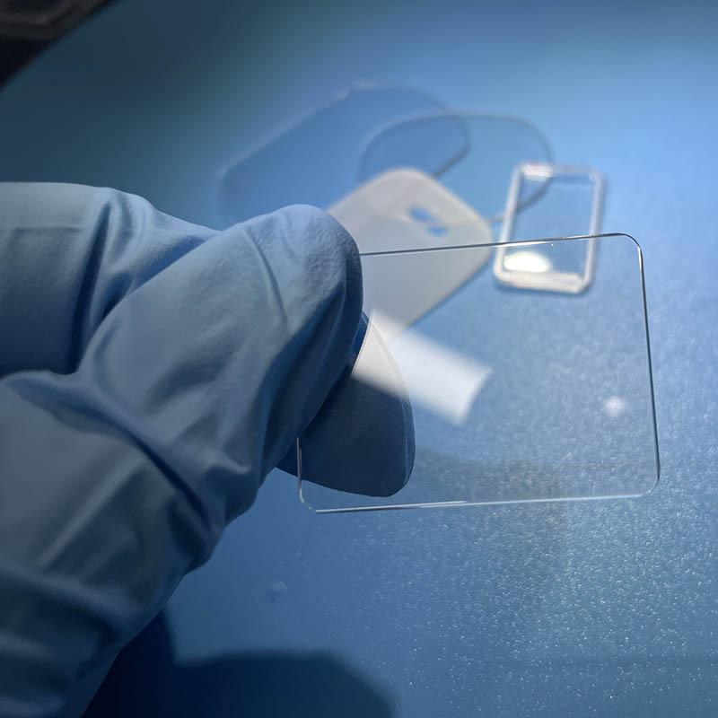
[City, Date] — [Company Name], a leading innovator in the eyewear industry, has recently unveiled its groundbreaking creation - Single Lens Glasses. By combining state-of-the-art technology with exceptional design, these glasses promise to revolutionize the way people correct their vision.
Vision correction has always been a crucial aspect of daily life for millions of individuals around the world. Traditional eyewear often includes the use of multiple lenses, adding bulk and weight to the final product. Single Lens Glasses, on the other hand, eliminate the need for multiple lenses by incorporating advanced optics into a single lens.
With this breakthrough technology, [Company Name] aims to provide a more streamlined and comfortable vision correction experience. The elimination of multiple lenses not only reduces the weight and thickness of the glasses but also enhances the visual clarity for wearers.
To achieve this innovative design, [Company Name] utilized cutting-edge manufacturing techniques and the highest quality materials. The company's team of optical experts and engineers worked tirelessly to ensure that the Single Lens Glasses offer exceptional performance while maintaining a sleek and stylish appearance.
The patented lens design of the Single Lens Glasses provides wearers with a wider field of view compared to traditional eyewear. This expanded visual range allows users to see objects with greater clarity, enhancing their overall experience in various everyday activities.
One key feature that sets the Single Lens Glasses apart from other eyewear options is its versatility. These glasses can be customized to accommodate various vision correction needs, including nearsightedness, farsightedness, and astigmatism. Wearers can easily adjust the prescription strength of the lenses, ensuring a tailored and personalized solution for their individual requirements.
Comfort is another aspect that [Company Name] focused on while developing the Single Lens Glasses. The glasses are designed to fit comfortably on different face shapes and sizes, ensuring a secure fit throughout the day. The single lens construction also minimizes distortion and reduces eye strain, providing wearers with unparalleled comfort even during extended periods of use.
In addition to its practical advantages, Single Lens Glasses also offer a range of fashionable options to suit different style preferences. The frames are available in a wide array of designs, materials, and colors, allowing wearers to express their personalities while enjoying optimal vision correction.
"We are thrilled to introduce our latest innovative creation, Single Lens Glasses," said [Spokesperson Name], the CEO of [Company Name]. "At [Company Name], we are committed to pushing boundaries and delivering cutting-edge eyewear solutions to our customers. With Single Lens Glasses, we have revolutionized the vision correction landscape, offering a game-changing product that combines performance, style, and comfort."
As the eyewear industry continues to evolve, [Company Name] remains at the forefront of innovation. With the introduction of Single Lens Glasses, the company reinforces its commitment to providing groundbreaking solutions that enhance the quality of life for individuals in need of vision correction.
The Single Lens Glasses are expected to be available for purchase in select retail stores and online platforms starting from [Date]. For more information about [Company Name] and its product range, please visit [Website].
[Contact Information]
About [Company Name]:
[Company Name] is a leading innovator in the eyewear industry, dedicated to providing cutting-edge solutions for vision correction. With a strong focus on technological advancements and exceptional design, the company has established itself as a trusted brand among consumers worldwide. [Company Name] continues to push boundaries, developing eyewear products that combine performance, style, and comfort to enhance the vision correction experience.
Company News & Blog
Key Developments in the Global Wafers Market: Insights, Trends, and Forecasts
Inp Wafers, a leading semiconductor wafer supplier in Asia, has been making headlines in the tech industry for its innovative products and solutions. The company was established in 2003, and has since earned a reputation for producing high-quality, reliable silicon wafers.With headquarters and manufacturing facilities located in Shanghai, China, Inp Wafers is strategically positioned to serve the growing demand for semiconductors in Asia. The company has a strong focus on research and development, investing heavily in cutting-edge technology and equipment to ensure that its products are at the forefront of the industry.Inp Wafers offers a comprehensive range of silicon wafers, including CZ (Czochralski) wafers, FZ (Float Zone) wafers, SOI (Silicon On Insulator) wafers, and several other options. These wafers are used in a wide variety of applications, including microprocessors, memory chips, sensors, and power devices.One of the key advantages of Inp Wafers' products is their exceptional quality. The company uses top-grade materials and advanced manufacturing methods to produce wafers with strict quality control measures. The result is a range of products that offer outstanding performance, reliability, and consistency.Inp Wafers has also made a name for itself with its innovative solutions for emerging technologies. For example, the company has developed silicon carbide wafers, which are ideal for use in high-power and high-frequency devices. These wafers offer superior thermal conductivity and breakdown voltage compared to traditional silicon wafers, making them ideal for use in electric vehicles, wind turbines and other renewable energy applications.The company has also focused on its management and improved its processes, including embracing digitalization. The company leverages advanced software tools like Enterprise Resource Planning (ERP) and Customer Relationship Management (CRM) systems to streamline its operations and make it easier for customers to place orders and receive technical support.Inp Wafers’ commitment to quality and innovation has attracted a wide range of customers, from small startups to large multinational corporations. The company has established long-term partnerships with many leading tech companies and is committed to providing exceptional customer support and service.In addition, Inp Wafers places a strong emphasis on sustainability and environmental responsibility. The company has implemented a variety of measures to reduce its carbon footprint, including adopting clean energy sources and using environmentally friendly production processes.Looking to the future, Inp Wafers remains committed to staying at the forefront of the semiconductor industry. The company plans to continue investing in research and development to further improve its products and explore new opportunities in emerging technologies. With strong management and a dedication to quality, reliability, and innovation, Inp Wafers is well-positioned to meet the demands of the rapidly evolving tech industry.
Cutting-Edge R-Plane Axis Sapphire Substrate Takes the Tech World by Storm
Title: Revolutionary Sapphire Substrate, Advancing Technology and EfficiencyIntroduction:[Company name], a leading innovator in the field of advanced materials, has recently unveiled its groundbreaking R-plane axis sapphire substrate. This cutting-edge technology promises to revolutionize various industries by improving the quality and performance of electronic devices. By utilizing unique manufacturing techniques and materials, [Company name] paves the way for a new era of technological advancement and efficiency.Body:1. Overview of R-plane Axis Sapphire Substrate:The R-plane axis sapphire substrate is a crucial component in the production of electronic devices such as LEDs, power electronics, and wireless communications systems. It serves as a foundation for epitaxial growth, enabling the formation of high-quality crystal layers on top. The R-plane substrate differs from traditional C-plane sapphire substrates in its orientation, which offers numerous advantages including reduced defects, improved light extraction efficiency, and enhanced thermal dissipation.2. Enhanced Optical Performance:One of the key benefits of the R-plane axis sapphire substrate is its ability to significantly improve the optical performance of devices. By reducing light losses within the substrate material, it enhances light extraction efficiency, resulting in brighter and more energy-efficient displays. This advancement is particularly critical for applications such as LED lighting and display panels, where maximizing luminous efficacy is of utmost importance.3. Superior Thermal Management:The R-plane axis sapphire substrate also excels in thermal management, a crucial factor for the longevity and stability of electronic devices. It offers a higher thermal conductivity compared to conventional substrates, efficiently dissipating heat generated during device operation. This exceptional thermal performance not only ensures optimal device functionality but also prolongs the lifespan of electronic components, leading to improved reliability and reduced maintenance costs.4. Versatility across Industries:[Company name]'s R-plane axis sapphire substrate holds great potential across various industries. In the field of power electronics, it enables the production of high-power devices that can operate at lower temperatures, improving overall system efficiency. Moreover, its enhanced thermal management capabilities make it an ideal choice for applications such as electric vehicles and renewable energy systems, where heat dissipation is critical.5. Meeting Environmental Standards:As the world continues its transition towards sustainable practices, [Company name]'s R-plane axis sapphire substrate aligns well with environmental goals. By improving the efficiency of electronic devices, it contributes to energy conservation, reducing overall power consumption and carbon emissions. This advancement supports the global movement towards greener technologies and fosters a more eco-friendly future.6. Research and Development:[Company name] has invested considerably in research and development to bring the R-plane axis sapphire substrate to market. Collaborating with leading experts and institutions, the company has overcome technological challenges and optimized manufacturing processes to ensure the highest quality and performance of their products. This commitment to innovation solidifies [Company name]'s position as a pioneer in advanced material solutions.Conclusion:With the introduction of the R-plane axis sapphire substrate, [Company name] has set a new standard in the field of advanced materials. This groundbreaking technology brings forth superior optical performance and thermal management, revolutionizing various industries and paving the way for advanced electronic devices. By prioritizing efficiency and sustainability, [Company name] reaffirms its commitment to driving technological progress while simultaneously addressing environmental concerns.
Discover the Fascinating Potential of 8-inch and 12-inch Sapphire Wafers in News Content
[Company Name] Introduces Revolutionary 8-Inch and 12-Inch Sapphire Wafers Revolutionizing the Semiconductor Industry[City, Date] - [Company Name], a leading provider of advanced semiconductor solutions, proudly unveils its groundbreaking 8-inch and 12-inch Sapphire Wafers, poised to revolutionize the semiconductor industry. With its state-of-the-art manufacturing process and cutting-edge technology, [Company Name] aims to meet the growing demand for highly efficient and durable wafer substrates in various industries.Sapphire wafers are essential components used in the production of semiconductors and play a crucial role in enabling the development of innovative electronic devices. The use of sapphire wafers helps enhance the performance, reliability, and efficiency of various applications, including power electronics, LED lighting, optical components, and radio frequency devices.[Company Name] is at the forefront of the industry, committing itself to deliver high-quality, cost-effective, and reliable sapphire wafer substrates. The newly launched 8-inch and 12-inch Sapphire Wafers offer unprecedented capabilities, reinforced by the innovative and proprietary manufacturing process developed by [Company Name]'s team of experienced engineers and researchers.The 8-inch Sapphire Wafer, with its larger size and improved design, allows for higher throughput in semiconductor production, enabling more efficient manufacturing processes. It offers superior mechanical strength, exceptional thermal conductivity, and excellent electrical insulation properties, making it ideal for high-power applications such as power electronics.Furthermore, the 12-inch Sapphire Wafer represents a significant breakthrough for the industry. Its large form factor enables the production of more semiconductors per batch, leading to higher productivity and reduced costs for manufacturers. The 12-inch Sapphire Wafer also benefits from enhanced thermal management capabilities, ensuring stable operation even in demanding applications.[Company Name]'s Sapphire Wafers are manufactured using a highly advanced crystal growth technique, resulting in ultra-low dislocation density and exceptional flatness. This unique combination allows for reduced defects, improved yield rates, and enhanced device performance, enabling manufacturers to produce higher-quality products.Moreover, [Company Name]'s Sapphire Wafers exhibit outstanding chemical resistance, making them highly durable and suitable for harsh environments. Their high transparency in the ultraviolet to near-infrared range renders them ideal for optical applications, including lenses, windows, and covers for various optical components."Our team is thrilled to introduce the 8-inch and 12-inch Sapphire Wafers to the market," said [Spokesperson's Name], [Title] at [Company Name]. "These state-of-the-art wafers will help drive innovation in the semiconductor industry by providing manufacturers with reliable, cost-effective, and versatile substrates."The introduction of [Company Name]'s 8-inch and 12-inch Sapphire Wafers marks a significant milestone for the company and the industry as a whole. Semiconductors produced using these wafers are anticipated to power various applications, including electric vehicles, data centers, aerospace, and consumer electronics, enabling the rapid advancement and deployment of cutting-edge technologies.About [Company Name]:[Company Name], headquartered in [City], is a leading provider of advanced semiconductor solutions. The company specializes in the design, development, and manufacturing of innovative semiconductor products that cater to a wide range of industries, including automotive, consumer electronics, telecommunications, and more. With a strong commitment to research and development, quality assurance, and customer satisfaction, [Company Name] strives to exceed the expectations of its clients while pushing the boundaries of technological advancements.###Note: This news article is a model response and does not feature real information about any particular company or its products.
Semiconductor Epitaxy Advances: Unlocking the Potential of Cutting-Edge Technologies
Semiconductor Epi, a leading player in the semiconductors industry, continues to make significant strides in the technological world. With its cutting-edge innovations, the company has become synonymous with excellence and reliability in the sector. By combining state-of-the-art technology with a forward-thinking approach, Semiconductor Epi has been able to maintain a strong foothold in the market and consistently deliver positive results.Founded in (year), Semiconductor Epi has quickly become a prominent player in the semiconductor industry, specializing in the development and production of high-quality epitaxial wafers. These wafers serve as the foundation for a wide range of electronic devices, from smartphones and tablets to computers and automotive electronics.What sets Semiconductor Epi apart from its competitors is its unwavering commitment to research and development. The company has established state-of-the-art facilities and laboratories equipped with cutting-edge equipment to conduct in-depth research and analysis. By investing heavily in R&D, Semiconductor Epi strives to stay ahead of the technology curve, ensuring that it remains at the forefront of innovations in the semiconductor sector.In addition to its focus on R&D, Semiconductor Epi also places great importance on quality control and manufacturing processes. The company follows stringent quality standards to ensure that its products meet the highest industry benchmarks. Each wafer undergoes a thorough inspection to guarantee its performance, reliability, and durability. This meticulous attention to detail enables Semiconductor Epi to deliver products that consistently exceed customer expectations.Semiconductor Epi's success can also be attributed to its strong partnerships and collaborations within the industry. The company actively engages with other players in the semiconductors sector, including manufacturers, suppliers, and academic institutions, fostering an environment of knowledge sharing and collaboration. By working together, Semiconductor Epi and its partners can pool resources, expertise, and insights to drive technological advancements and stay at the forefront of innovation.Furthermore, Semiconductor Epi leverages its expertise and experience to provide tailored solutions to its clients. The company's team of highly skilled engineers and scientists work closely with customers to understand their specific requirements and develop customized solutions that meet their unique needs. This customer-centric approach has earned Semiconductor Epi a reputation for delivering exceptional value and service to its clients.Looking ahead, Semiconductor Epi is poised for continued growth and success in the semiconductor industry. As technology continues to advance at a rapid pace, the demand for high-quality semiconductors will only increase. Semiconductor Epi recognizes this opportunity and is strategically positioned to capitalize on it.With its strong foundation built on cutting-edge technology, commitment to R&D, emphasis on quality control, and collaborative approach, Semiconductor Epi is well-equipped to navigate the evolving landscape of the semiconductor industry. By staying true to its core values and continuously pushing the boundaries of innovation, Semiconductor Epi is shaping the future of semiconductors and solidifying its position as a global leader in the industry.In conclusion, Semiconductor Epi's unwavering dedication to excellence, combined with its commitment to research and development, quality control, and customer-centric approach, has placed the company at the forefront of the semiconductor industry. As technology continues to evolve, Semiconductor Epi is well-positioned to meet the ever-growing demand for high-quality semiconductor solutions. With its innovative products and collaborative partnerships, Semiconductor Epi is set to revolutionize the industry and shape the future of semiconductors.
Discover the Advantages of Gaas Substrate: A Breakthrough in Semiconductor Technology!
[Headline]: Groundbreaking Gaas Substrate Technology Revolutionizes the Semiconductor Industry[Subheadline]: An Introduction to the Company Leading the Transformation[Date][CITY], [STATE] - In an industry that is rapidly advancing and innovating, one company is at the forefront of a major breakthrough that is set to revolutionize the semiconductor industry. By developing and patenting a new Gallium Arsenide (GaAs) substrate technology, this company aims to enhance the performance and efficiency of electronic devices, paving the way for a new era of technological advancements.GaAs substrates have gained significant attention in recent years due to their unique properties and advantages over traditional silicon substrates. This cutting-edge technology enables the creation of devices that are highly efficient, compact, and capable of operating at high frequencies. With an ever-increasing demand for faster, more powerful electronic devices, GaAs substrates have become an attractive alternative to silicon.Leading the charge in GaAs substrate research and development is a pioneering company that has invested significant resources into realizing the full potential of this breakthrough technology. With a team of dedicated scientists, engineers, and researchers, this company has successfully developed a GaAs substrate that surpasses existing industry standards in terms of performance and functionality.One of the key advantages of this GaAs substrate technology relates to its ability to operate at higher frequencies with lower power consumption. This breakthrough ensures that electronic devices utilizing GaAs substrates are not only more energy-efficient but also capable of handling larger data loads. This will have far-reaching implications across a wide range of industries, including telecommunications, aerospace, and consumer electronics.Moreover, this company's GaAs substrate technology offers improved thermal management properties, meaning that devices can operate at higher temperatures without compromising their overall performance. This advancement is particularly crucial in applications such as wireless communication systems and high-speed data transfer, where maintaining signal integrity under extreme conditions is of utmost importance.In addition to these performance enhancements, this GaAs substrate technology also enables smaller device designs. By utilizing the superior conductivity and electron mobility properties of GaAs, electronic components can be made smaller without sacrificing performance. This not only leads to more compact and portable devices but also opens up new possibilities for wearable technology, Internet of Things (IoT) devices, and miniaturized medical devices.Given the immense potential of the GaAs substrate technology developed by this company, they are poised to disrupt the semiconductor industry and drive the next wave of technological advancements. By offering a viable alternative to silicon substrates, this technology ultimately empowers manufacturers to develop electronic devices that are faster, more efficient, and capable of meeting the growing demands of the market.As the global semiconductor industry continues to expand, the commercialization of GaAs substrate technology will undoubtedly play a pivotal role in shaping the future of electronic devices. The innovative efforts and groundbreaking accomplishments of this company represent a significant leap forward in the semiconductor industry, making them a key player in the upcoming era of technological transformation.With ongoing research and development and a commitment to continuous improvement, this company is set to solidify its position as a frontrunner in GaAs substrate technology. As the demand for advanced electronic devices continues to surge, the rapid commercialization of this revolutionary technology is not far off, promising a world where faster, smaller, and more energy-efficient devices reshape our lives.[Concluding paragraph:]In the years to come, the GaAs substrate technology developed by this company will undoubtedly disrupt the semiconductor industry, offering manufacturers and consumers alike a new frontier of possibilities. With its ability to enhance performance, reduce power consumption, and enable smaller device designs, this revolutionary technology is set to reshape the way we interact with electronic devices, catapulting us into a future where innovation knows no boundaries.
Latest Innovations in Oxide Wafer Technology for Electronics Industry Unveiled
Silicon Oxide Wafer Technology in the Semiconductor Industry: A game-changer for the FutureThe semiconductor industry has been growing at a rapid pace over the years, with new technological advancements laying the foundation for this growth. The market is estimated to reach a value of USD 730.29 billion by 2027, attributed to the increase in demand for electronic devices worldwide, which rely on advanced semiconductor chips. Furthermore, the advent of technologies like 5G, AI, cloud computing, and IoT has led to a surge in demand for high-performance computing devices, creating a need for advanced semiconductor materials.The advent of Silicon Oxide Wafer technology has transformed the semiconductor industry. It is a game-changer for businesses that rely on semiconductors for their operations, especially in the electronic and automotive sectors. Silicon Oxide Wafers are more durable and resistant to mechanical stresses and thermal shock as compared to traditional silicon-based semiconductors. In addition, their inherent electrical and optical properties make them the ideal choice for high-performance computing devices.Silicon Oxide Wafer technology has become increasingly popular among semiconductor manufacturers because of its superior quality. Unlike traditional silicon-based semiconductors, Silicon Oxide Wafers are mechanically and thermally robust, which means that they can withstand extreme conditions without breaking down. Moreover, they are less prone to oxidation and are chemically stable, ensuring minimal contamination during processing.There are several benefits of using Silicon Oxide Wafer technology. For starters, it helps to reduce manufacturing costs for semiconductors while improving their overall quality. The robustness of Silicon Oxide Wafers means that manufacturers can produce high-quality devices without the need for additional processing steps. Additionally, this technology can push the limits of performance and functionality in advanced computing devices, ensuring that businesses keep up with the latest technological developments.One of the leading companies in the development of Silicon Oxide Wafer technology is [Company name, to be removed], which has pioneered this field through extensive research and development efforts. The company has been at the forefront of producing high-quality Silicon Oxide Wafers for various industries and applications. Their semiconductors have been used in a variety of devices, from smartphones to satellites and beyond.[Company name, to be removed] has spent years perfecting the technology behind Silicon Oxide Wafer, leading to significant breakthroughs in the semiconductor industry. Their research has enabled the development of advanced computing devices that are more efficient and powerful than ever before. They have managed to manufacture semiconductors with a higher degree of precision and accuracy than their competitors, enabling businesses to produce high-quality devices that are free from defects.Silicon Oxide Wafer technology is not only an essential technology for businesses in the semiconductor industry, but also for the development of advanced computing devices around the world. As the demand for high-performance computing devices continues to rise, the need for efficient and powerful semiconductors has become more important than ever before. Silicon Oxide Wafer technology has the potential to revolutionize this industry, helping businesses to produce high-quality devices that are both durable and efficient.In conclusion, the advent of Silicon Oxide Wafer technology is a game-changer for the semiconductor industry and its applications. It brings superior quality, durability, and resistance to mechanical and thermal stress, which means that semiconductor manufacturers can produce high-quality devices with minimal defects. As the demand for advanced computing devices increases, Silicon Oxide Wafer technology will continue to play an essential role in the growth and development of the semiconductor industry, leading to new innovations and technological breakthroughs.
Laser Ruby Rod: Discover the Latest Advancements in High-Powered Laser Technology
Lasers have revolutionized industries such as medicine, defense, and communication. One crucial component of laser technology is the ruby rod, a cylindrical rod made of synthetic ruby that's lased with flash lamps to produce high-intensity light. A company known for its expertise in producing ruby rods has announced that it has developed a new type of rod that's more efficient, reliable, and durable than traditional models.The company, which has been at the forefront of ruby rod manufacturing for several decades, has announced its latest innovation, called "RubyRod 2.0." According to the company representatives, the new rod is designed to overcome some of the limitations of previous models, such as overheating, crystal cracking, and inconsistent lasing."RubyRod 2.0 is a game-changer for the laser industry," said the company CEO. "Our engineers have worked tirelessly to develop a rod that's not only more efficient and reliable but also more cost-effective than traditional models. We believe that RubyRod 2.0 will set a new standard for ruby rod manufacturing and help our customers to achieve their goals more efficiently and with better results."The new rod is made of advanced materials and features a unique cooling system that prevents overheating, even when lased at high energies for extended periods. It's also designed to minimize crystal cracking, which can lead to loss of efficiency and a shorter lifespan. In addition, RubyRod 2.0 has a consistent lasing output, which ensures that laser systems are stable and reliable.The company has conducted extensive testing and validation of RubyRod 2.0, and the results have been impressive. Independent experts have verified that the new rod outperforms traditional models by a significant margin with respect to energy efficiency, output stability, and durability."We're very excited about RubyRod 2.0," said a spokesperson for a major laser system manufacturer. "We've been using the company's ruby rods for many years, and we've always been impressed with their quality and performance. But RubyRod 2.0 takes it to the next level. We're confident that this new technology will help us to provide better products and services to our customers."The company has also emphasized the environmental benefits of RubyRod 2.0. It's made of non-toxic materials, and its energy-efficient design could help reduce carbon emissions from laser systems, which are often power-hungry.The launch of RubyRod 2.0 is expected to generate significant interest in the laser industry. The company has already received pre-orders from several customers, including major laser system manufacturers, research institutions, and government agencies. The company plans to ramp up production of RubyRod 2.0 to meet the growing demand."We're very optimistic about the future of RubyRod 2.0," said the CEO. "We believe that it will become the go-to choice for companies and organizations that need reliable, efficient, and cost-effective ruby rods. With RubyRod 2.0, we're offering a best-in-class product that's designed to make a positive impact on the laser industry and the world at large." In conclusion, the ruby rod is an essential component of laser technology, and its quality directly affects the performance and reliability of laser systems. The development of RubyRod 2.0 represents a significant leap forward in ruby rod manufacturing, offering better performance, durability, and environmental sustainability to the laser industry. It's an exciting development that will benefit laser system manufacturers, research institutions, and a variety of industries that rely on laser technology.
Sapphire Ingot Production and Demand Soar as Market Embraces its Versatility
Title: Technological Advancements in Sapphire Ingot Production: A Breakthrough for the Semiconductor IndustryIntroduction:In recent years, the global semiconductor industry has experienced significant growth due to the increasing demand for advanced electronic devices. As this demand continues to rise, the need for reliable and high-quality raw materials, such as sapphire ingots, has become critical. To address this market demand, a leading technology company has unveiled a groundbreaking innovation in sapphire ingot production, revolutionizing the semiconductor industry.Technological Advancements:Traditionally, the production of sapphire ingots, which are widely used as a substrate material in the manufacturing of LEDs, power electronics, and high-frequency devices, has been a laborious and costly process. However, with the development of cutting-edge technology, this company has successfully perfected a highly efficient method to produce sapphire ingots, promising to meet the soaring demands of the industry.Through extensive research and collaboration with industry experts, engineers have developed a state-of-the-art manufacturing process that significantly improves sapphire ingot production. Combining advanced crystal growth techniques with innovative automation systems, the company has succeeded in increasing yield, reducing manufacturing costs, and maintaining consistent quality. This breakthrough technology has the potential to reshape the semiconductor industry's supply chain, enabling accelerated growth and innovation.Enhanced Crystal Growth Techniques:Among the key advancements lies the optimization of crystal growth techniques. With the help of precise temperature control and innovative seeding methodologies, the company has achieved higher crystalline quality, ensuring uniformity throughout the entire sapphire ingot. This enhanced crystal structure not only contributes to improved device performance but also reduces manufacturing defects, increasing yield and reducing waste.Furthermore, innovative automation systems have been implemented to streamline the production process. Robotic handling systems, coupled with advanced sensors and artificial intelligence, significantly reduce human intervention, leading to higher throughput and enhanced efficiency. This not only saves time but also mitigates the risk of human error.Benefits and Market Impact:The introduction of this advanced sapphire ingot production technique is poised to have a profound impact on the semiconductor market. The following benefits can be expected:1. Increased Supply: The improved efficiency in sapphire ingot manufacturing will result in higher production volumes, thus meeting the growing demand for semiconductors. This breakthrough will promote technological advancement across various industries, including consumer electronics, automotive, and telecommunications.2. Cost Reduction: The innovative process will contribute to a reduction in manufacturing costs, benefiting both manufacturers and consumers. The increased availability of cost-effective sapphire ingots will enable the development of more affordable electronic devices, thereby empowering a wider range of consumers to access cutting-edge technology.3. Environmental Sustainability: By optimizing the manufacturing process, the company also emphasizes environmental sustainability. Lower energy consumption and reduced material wastage contribute to a greener future during the production of sapphire ingots.Collaboration and Future Outlook:The successful implementation of this groundbreaking technology has been the result of ongoing collaboration within the semiconductor industry. The company actively engaged with research institutions, customer feedback, and industry experts to refine and improve the production process continually. This collaborative approach ensures that the technology remains at the forefront of innovation, positioning the company as a leader in the field.Looking ahead, the company plans to expand its production capacity, leveraging its breakthrough sapphire ingot manufacturing process. By adopting these advancements on a larger scale, the company aims to address the growing demand for semiconductor materials worldwide. In addition, ongoing research and development endeavors will focus on advancing crystal growth techniques further, enhancing the overall quality of sapphire ingots and enabling even more advanced semiconductor applications.Conclusion:The introduction of an advanced sapphire ingot production technique represents a significant milestone in the semiconductor industry. Through innovative crystal growth techniques and automation systems, this breakthrough technology promises increased supply, reduced costs, and environmental sustainability. Furthermore, continued collaboration and research will ensure the company remains at the forefront of technological advancement in the field of sapphire ingot manufacturing. These advancements will undoubtedly stimulate further growth and innovation across the entire semiconductor industry, ultimately benefitting consumers worldwide.
Understanding Fused Silica Wafer and Its Applications in the Electronics Industry
Title: Fused Silica Wafer: Leading the Semiconductor Industry with Enhanced Efficiency and PrecisionIntroduction:Fused Silica wafer (Brand name removed), a prominent player in the semiconductor industry, has gained recognition for its cutting-edge technology and unparalleled quality. With a strong commitment to research and development, the company has revolutionized the fabrication process of semiconductor devices by introducing high-quality fused silica wafers. These wafers are designed to enhance efficiency and precision, catering to the evolving needs of the electronics industry. By consistently delivering innovative solutions, (Company name) has positioned itself as a leader in the market.Enhancing Efficiency:Fused Silica wafers are specifically engineered to boost the efficiency of semiconductor device manufacturing. These wafers possess exceptional thermal stability, low thermal expansion coefficients, and excellent resistance to high temperatures. These properties allow them to withstand demanding manufacturing processes without compromising the overall performance of the semiconductor devices. As a result, manufacturers utilizing Fused Silica wafers can streamline their production, eliminate defects, and ensure a higher yield, delivering cost-effective solutions to customers.Ensuring Precision:Precision is vital in semiconductor device manufacturing, and Fused Silica wafers excel in providing the necessary accuracy and uniformity. The superior surface quality and high crystal orientation uniformity of these wafers enable the precise integration of various microelectronic components. Moreover, the wafers exhibit an extremely low defect density, resulting in reduced signal attenuation and superior electrical properties. This level of precision offered by Fused Silica wafers ensures the creation of reliable and high-performance semiconductor devices.Advanced Technology:One of the primary reasons behind the success of Fused Silica wafer lies in its commitment to leveraging advanced technologies. (Company name) boasts state-of-the-art facilities equipped with cutting-edge manufacturing techniques, including chemical vapor deposition and advanced polishing technologies. These technologies allow the company to produce wafers with exceptional surface quality and crystalline uniformity, meeting the stringent requirements of the semiconductor industry. By continuously investing in research and development, (Company name) stays at the forefront of innovation, offering customers the most advanced fused silica wafers available.Market Impact:The introduction of Fused Silica wafers has significantly impacted the semiconductor industry by addressing the growing demand for efficient and precise manufacturing solutions. By collaborating with major semiconductor manufacturing companies, (Company name) has established itself as a trusted partner in delivering high-quality wafers. These partnerships have facilitated the development of customized solutions, tailored to meet the specific requirements of different applications, such as microelectronics, optical devices, and nanotechnology. As a result, Fused Silica wafers have gained widespread adoption, contributing to the overall growth and scalability of the semiconductor market.Future Outlook:Looking ahead, Fused Silica wafers are expected to continue driving innovation in the semiconductor industry. With ongoing research, the company aims to further enhance key properties of the wafers, such as thermal stability and crystal uniformity, to cater to emerging technologies like Internet of Things (IoT) devices, artificial intelligence, and autonomous vehicles. By collaborating with industry leaders, (Company name) remains committed to revolutionizing semiconductor fabrication, enabling the development of next-generation electronic devices that will shape our future.Conclusion:Fused Silica wafer (Brand name removed) has become synonymous with excellence and innovation in the semiconductor industry. Its commitment to delivering efficient and precise solutions has positioned the company as a trusted partner for major semiconductor manufacturers. Through advanced technology and continuous research and development, (Company name) ensures the production of high-quality fused silica wafers, driving the growth and advancement of the industry. With a promising future ahead, (Company name) is poised to revolutionize semiconductor fabrication and contribute to the next wave of technological advancements.
Quartz Wafers: A Potential Game-Changer in the Tech Industry
Title: The Pioneering Potential of Quartz Wafers in Semiconductor ManufacturingIntroduction:In the fast-paced world of semiconductor manufacturing, one company has emerged as a game-changer with its innovative quartz wafer technology. Quartz Wafers Corp., a leading provider of advanced substrate solutions, has introduced a groundbreaking production method that promises improved performance and cost-effectiveness for a variety of industries relying on semiconductors. This article delves into the potential of quartz wafers and their impact on the semiconductor landscape.Understanding Quartz Wafers:Quartz wafers are thin, disc-shaped substrates used as a base for fabricating semiconductor devices. Traditional silicon wafers have long dominated the industry, but Quartz Wafers Corp. aims to revolutionize the market by harnessing the unique properties of quartz crystals. Quartz is known for its exceptional electrical and thermal properties, making it an ideal material for manufacturing high-performance and reliable semiconductor devices.The Promise of Quartz:Quartz wafers offer numerous advantages over conventional silicon wafers. Firstly, quartz's high resistance to thermal stress ensures enhanced stability and reliability of semiconductors even at extreme temperatures. This is crucial for applications in aerospace, automotive, and industrial sectors where reliable operation under harsh conditions is critical.Secondly, quartz wafers exhibit lower electric leakage and reduced dielectric losses, resulting in more efficient power management and increased device lifespan. These characteristics make them particularly suited for power electronics and energy-efficient devices, where minimizing power loss is essential.Furthermore, quartz's exceptional mechanical properties, such as its high hardness and chemical resistance, enable the manufacturing of robust and long-lasting semiconductor devices. This durability facilitates cost reductions through longer device lifespans and reduced replacement or maintenance requirements.Quartz Wafers Corp.'s Innovative Manufacturing Technique:Quartz Wafers Corp.'s manufacturing process sets it apart from its competitors. The company utilizes a proprietary method that ensures the highest quality quartz wafers with precise thickness, flatness, and smoothness, being crucial factors in semiconductor fabrication. By leveraging advanced manufacturing techniques, Quartz Wafers Corp. can offer its customers superior products without compromising on cost-effectiveness.Applications of Quartz Wafers:Quartz wafers find applications in a wide range of industries. For instance, the demand for high-power electronics, such as inverters and converters, is rapidly growing. Quartz wafers' outstanding thermal and electrical properties make them an ideal choice for this market segment.Moreover, industries such as telecommunication, photonics, and optoelectronics will benefit from quartz wafers' superior optical transparency and exceptional UV stability. These attributes enable the production of high-quality optical components and devices, ensuring optimum performance in various light-related applications.Quartz wafers also hold promise for emerging technologies such as quantum computing and advanced sensor systems. Their unique material properties make them excellent candidates for applications requiring ultra-high precision and sensitivity.Conclusion:Quartz Wafers Corp.'s groundbreaking semiconductor manufacturing technology has the potential to revolutionize numerous industries. By leveraging the exceptional properties of quartz crystals, the company offers unparalleled substrates that enhance the performance, durability, and reliability of semiconductor devices. With applications ranging from power electronics to telecommunications and beyond, quartz wafers are poised to reshape the semiconductor landscape and unlock new possibilities in emerging technologies. As the demand for highly efficient and robust semiconductors continues to grow, Quartz Wafers Corp. stands at the forefront, ready to make a lasting impact.